
 |
|
Biography
Michael Waltl was born in Oberndorf near Salzburg, Austria. He received the BSc degree in electrical engineering and the degree of Diplomingenieur in microelectronics from the Technische Universität Wien in 2009 and 2011, respectively. He joined the Institute for Microelectronics in January 2012, where he is currently working on his doctoral degree. His scientific interests include negative and positive bias temperature instabilities and electric measurement methods.
Single-Trap Study of PBTI in SiON NMOS Transistors Using the Time-Dependent Defect Spectroscopy
Recent progress in semiconductor device technology has lead to nano-scale Metal-Oxide-Semiconductor Field Effect Transistors (MOSFETs). As a consequence, reliability issues, such as the Bias-Temperature Instability (BTI), have become more pronounced, thus attracting the interest of the semiconductor community. BTI is observed in pMOSFETs and nMOSFETs when a positive/negative gate voltage stress (PBTI/NBTI) is applied and seriously affects the MOSFET lifetime.
So far, most studies have focused on NBTI in SiON pMOSFETs as well as on PBTI/NBTI in high-k gate stacks. There is only a very small number of studies focusing on PBTI in SiON nMOSFETs, which is weaker by one order of magnitude compared to NBTI. However, in order to complete our microscopic understanding of the phenomenon, it is mandatory to investigate this effect as well.
To study the nMOSFETs recovery behavior ensuing right after the termination of gate bias stress, we used the recently proposed Time-Dependent Defect Spectroscopy (TDDS) to gain detailed insight into single-defect statistics. In nano-scale devices, the recovery proceeds in discrete steps. Quite to the contrary, in large area devices the recovery is continuous. This is due to the fact that the step heights are inversely scaled with the gate area. As a consequence, the single trapping events can hardly be separated. Therefore, a sophisticated experimental setup had to be developed to characterize defects in large-area nMOSFETs. At the same time, the nMOSFETs have a trap density of approximately ten percent of that in pMOSFETs. Therefore, the selection of nMOSFETs is limited to large-area devices showing smaller discrete trapping, see recovery traces from Fig. 1.
Recent measurements from an 0.16μm x 2μm nMOSFETs demonstrate that similarly to pMOSFETs, bias-dependent and bias-independent emission times are observed. Whereas bias-dependent emission time can be linked to switching-trap behavior, the bias-independent emission times correspond to fixed-oxide traps. During the last couple of years, the four state Non-radiative MultiPhonon (NMP) model, which can describe the capture and emission behavior of hole trapping observed in NBTI/pMOSFET experiments, has been developed. Using our recent data, we could demonstrate that the four-state NMP model can also explain electron trapping in PBTI/nMOSFET experiments.
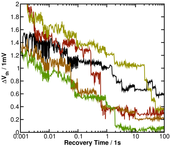
Fig. 1: Five selected recovery traces with each discrete step corresponding to the emission of a single electron. The traces are recorded on an 0.16μm x 2μm nMOSFET device after BTI stress with a stress time 100s and at stress voltage of 2.2V. As clearly visible, for the investigated device the heights of the discrete steps are in the range of approximately 0.2mV and lower, a consequence of the relatively large device area.
