
 |
|
Biography
Thomas Windbacher was born in Mödling, Austria, in 1979. He studied physics at the Technische Universität Wien, where he received the degree of Diplomingenieur in October 2006. He joined the Institute for Microelectronics in October 2006 and finished his doctoral degree on engineering gate stacks for field-effect transistors in 2010. From 2010 until the beginning of 2012 he worked as a patent attorney candidate in Leoben. In March 2012 he rejoined the Institute for Microelectronics, where he currently works on the modeling and simulation of magnetic device structures.
Spintronic Building Blocks: Towards Fully Non-Volatile Information Processing Systems
The seemingly endless demand for cheap electronics propelled scaling efforts in Complementary Metal-Ooxide-Semiconductor (CMOS) technology from the very beginning. CMOS device dimensions have advanced to a level where physical limitations and the ever increasing costs related to manufacturing the next technology node will soon bring further progress to a halt. At the same time, properties like power consumption, interconnection delay, durability, fast operation, long retention times, etc., have gained successively in weight.
Therefore, it is necessary to investigate alternative materials, devices, and computational principles to ensure future progress. Here, spin as a degree of freedom receives special attention due to its non-volatility, high endurance, and fast operation. However, the transition towards non-volatility comes at a price. All basic electronic building blocks have to be reevaluated and redesigned to harvest the maximum profit from the peculiarities of spintronics.
For instance, even though non-volatile flip flops based on CMOS/Magnetic Tunnel Junction (MTJ) hybrid circuits already perform quite well compared to pure CMOS solutions with respect to power and speed, their integration density is — up to now — still poor. This is caused by the intrinsic mismatch between the CMOS signal domain (voltage, charge) and the micro magnetic signal domain (spin transfer torque, resistance). Thus, additional transistors are needed to convert the signal between the two domains every time information is read, written, or processed, leading more likely to an integration density decrease than freeing die space.
Therefore, we proposed a non-volatile magnetic flip flop, which does not use MTJs solely as auxiliary memory elements, but instead performs everything in the magnetic domain. The result is a flip flop that takes advantage of the beneficial features of spintronics and simultaneously exhibits a very small footprint. Fig. 1 shows the structure of the proposed non-volatile magnetic flip flop.
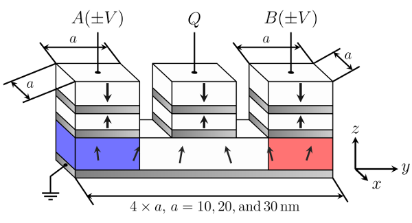
Fig. 1: Shows the proposed non-volatile magnetic flip flop comprising a shared free layer, which stores the information via the magnetization orientation, two stacks A,B for input and one stack Q for output. The current (voltage) polarities and the magnetization orientation of the free layer are mapped to logic 0 and 1. Applying synchronously two identical input polarities at A and B writes either logic 0 or 1 into the shared free layer (SET and RESET), while two input pulses with opposing polarities do not change the orientation of the shared free layer (HOLD).
