 |
|
Biography
Alexander Grill studied Microelectronics at the Technische Universität Wien, where he recieved his Diplomingenieur degree in 2013. Since March 2013 he is working on his doctoral degree at the Institute for Microelectronics. His scientific interests are the simulation of nitride-based heterostructure devices.
Single-Defect Characterization in GaN/AlGaN Fin-MIS-HEMTs
In comparison to conventional transistors, superior electronic properties, like high breakdown voltage, low on-state resistance and high switching frequency, make gallium-nitride (GaN)/aluminum-gallium-nitride (AlGaN) high-electron-mobility transistors (HEMTs) promising candidates for high-power and high-frequency devices. Recently, a promising approach to creating normally-off devices, which are essential for switching applications, was presented by using nanosized fin-MIS-HEMT structures. Nonetheless, despite all these recent improvements, charge trapping remains a severe reliability issue in GaN devices.
Unfortunately, due to complicated electrostatics and relatively high defect densities, experimental characterization of the responsible defects proves extremely challenging. One reason for this is that only ensembles containing a large number of defects can be assessed by measurement in large area devices. Broad distributions of capture and emission times and Coulomb feedback of the traps further complicate the analysis of individual trap properties. To gain better insight into the physical mechanisms of charge trapping and the nature of the defects involved, nanoscale devices are very promising because they enable the investigation of individual single-defect properties.
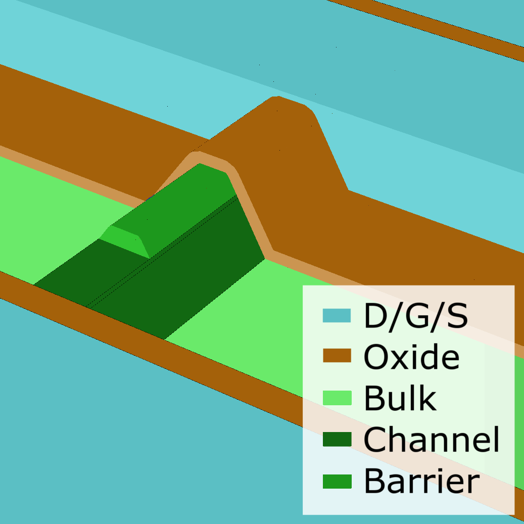
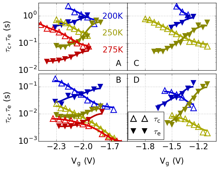
To study charge trapping at the single-defect level, we probed a 50 nm x 1 μm fin-MIS-HEMT, as shown in Fig. 1. We were able to identify four defects producing correlated random telegraph noise (RTN) using our TDDS measurement instrument (TMI). In order to extract their defect properties, we collected charge capture and emission events across several voltages and temperatures. The bias and temperature dependence of the four extracted defects is given in Fig. 2. Given the voltage and temperature behavior of the four individual defects, we were able to extract their vertical position, as well as their trap level, using a two-state non-radiative multi-phonon (NMP) model.
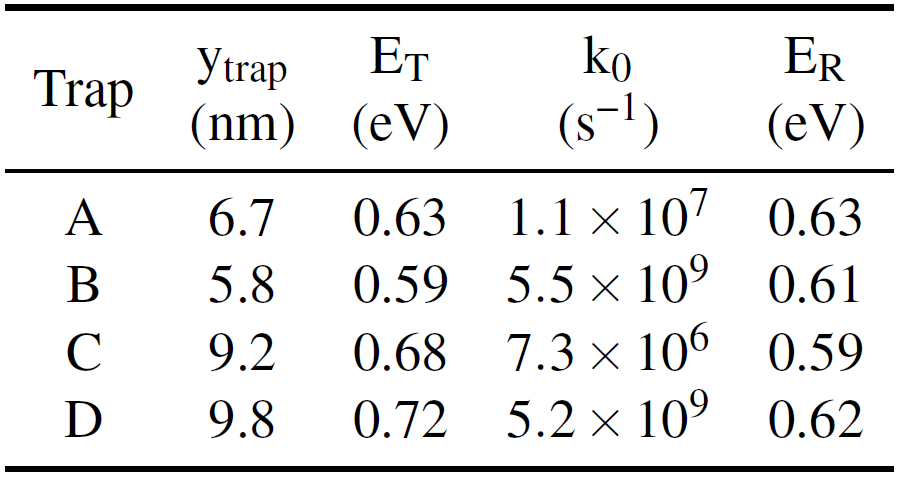
The results of the parameter extraction of all four defects are given in the table in Fig 3. The trap positions of the correlated trap pairs, "AB" and "CD", are in close vicinity to each other. Since the intersection points also match, they share a similar trap level, although their absolute time constants have a difference of at least one order of magnitude. The relaxation energy of the NMP process can be calculated from the activation energy extracted from the Arrhenius plot (not shown).
One possible explanation for the observed behavior, namely (a) the correlated RTN behavior, (b) the similar trap levels and (c) the similar voltage behavior, could be the local surroundings seen by defects "B" and "D", which apparently change when defects "A" and "C" capture a charge.

Fig. 1: The simplified device geometry used for our simulations. A 30 nm thick AlGaN barrier is placed on top of an 80 nm thick GaN channel layer. The thickness of the Al2O3 gate oxide is 20 nm and the fin length is 1 μm.

Fig. 2: The weak voltage dependence of the capture times of the four individual defects suggests a defect location close to the channel. Further evidence for this assumption is given by the fact that RTN occurs at negative gate voltages, where electron trapping by oxide defects through the barrier is very unlikely. The defect pairs share the same intersections and voltage dependence, suggesting a strong electrostatic coupling.

Fig. 3: The defect properties extracted from Fig. 6. The extracted trap levels of the defect pairs match closely, confirming their similar positions within the barrier. Their similar intersections, their voltage dependence and their correlated behavior suggest that the potential energy surface around defects "B" and "D" changes when defects "A" and "C" have captured an electron.


