 |
|
Biography
Theresia Knobloch was born in Vienna in 1992. She received her BSc degree in Technical Physics and the degree of Diplomingenieur in Microelectronics from the Technische Universität Wien in 2014 and 2016, respectively. She joined the Institute for Microelectronics in April 2016, where she is currently working on her doctoral degree. Her current research topic are novel devices based on two-dimensional materials.
Physical Modeling of Hysteresis in MoS2 Field-Effect Transistors
Research into two-dimensional materials has seen an exponential increase during the last decade, triggered by the discovery of the electric field effect in graphene in 2004. However, graphene lacks a band gap which leads to a very low current on/off ratio, making it unsuitable for digital circuits. Attention has therefore gradually shifted to other two-dimensional materials possessing a band gap, such as molybdenum disulphide (MoS2), a member of the large group of transition metal dichalcogenides.
Since the first practical realization of a field-effect transistor (FET), based on one atomic monolayer of MoS2 in 2011, many research groups have succeeded in fabricating these devices. Although these devices showed promising properties, they have still not met the high expectations. Apart from a carrier mobility that does not exceed the order of 100 cm2V-1s-1, widely known reliability issues, such as hysteresis commonly observed in gate-transfer characteristics, have severely inhibited industrial applications of these novel devices. We have therefore developed a physical modeling approach for describing hysteresis in MoS2-based FETs. In this way, we have arrived at an enhanced understanding of this phenomenon, which may help to mitigate the hysteresis problem in the future.
Our approach consists of a drift-diffusion-based TCAD model coupled to a full four-state non-radiative multiphonon (NMP) model, used to describe charge capture and emission events in the gate dielectric. The drift-diffusion equations are computationally very efficient and entirely sufficient for describing charge transport through the channel of large-area MoS2 FETs. The four-state NMP model was previously developed for describing charge capture and emission events in silicon dioxide (SiO2), which causes bias temperature instabilities (BTI) in silicon-based devices.
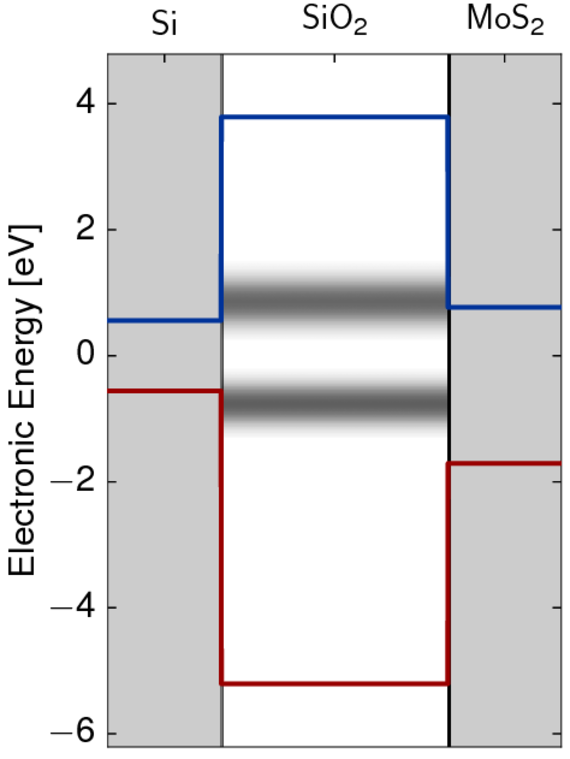
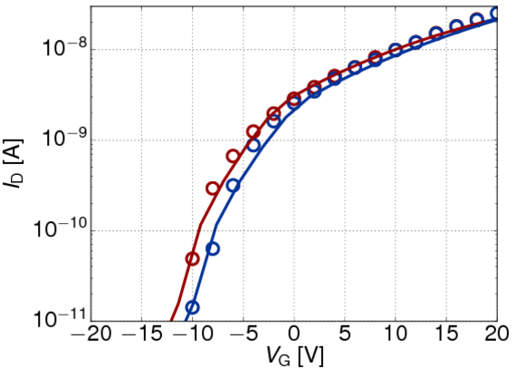
This model has now been applied and calibrated to novel MoS2 devices. The degradation in these devices is governed by a defect band located at approximately 2.9 eV below the conduction band edge of SiO2, which is illustrated in Fig. 1. Simulations performed with this setup could accurately capture hysteresis in gate-transfer characteristics (see Fig. 2). This is a strong indication that charge capture and emission processes are in fact one of the main reasons for the hysteresis
observed in MoS2 FETs.

Fig. 1: Band alignment of the band gap in silicon to the band gap in one monoatomic layer of MoS2 and to the defect bands in SiO2. The upper band dominates the degradation in MoS2 FETs, while the lower defect band is responsible for BTI in silicon-based devices.

Fig. 2: Comparison of measured and simulated hysteresis in the gate-transfer characteristics of one device. The characteristics were captured using a sweep time of T = 1/f = 80 s.


