 |
|
Biography
Alexander Makarov was born in Volgograd, Russia, in 1985. He studied information technology at the Volgograd State Technical University, where he received the BSc degree in 2006 and MSc degree in 2008. He joined the Institute for Microelectronics in October 2009 and has obtained the doctoral degree in March 2014. He is currently employed as a post-doc researcher. His scientific interests include Monte-Carlo simulations and nonvolatile memory device modeling.
Spin-Orbit Torque MRAM Based on Cross-Point Architecture
Three-terminal memory cell structures based on a magnetic tunnel junction (MTJ) are promising candidates for future generations of MRAM. Spin-orbit torque (SOT) based magnetization manipulation is suitable for the development of three-terminal MRAM cells because the switching current does not flow through the barrier layer.
Typically, an SOT-MRAM cell is an MTJ fabricated on a heavy metal channel with a large spin Hall effect (SHE)/spin-orbit interaction, wherein the free layer is in direct contact with the heavy metal channel. Spin torque is induced by the in-plane current through the SHE and/or the interfacial spin-orbit coupling. An external magnetic field is required to switch MTJs with perpendicular magnetization and in-plane structures with the magnetization parallel to the current as it breaks the symmetry in response to the spin torque and provides the deterministic switching.
Recently, switching has been demonstrated in MTJs fabricated on Ta-, W- and Ir-doped Cu. SOT-MRAM exhibits faster switching than structures with spin-transfer torque switching. On the other hand, a typical spin-orbit-based memory takes more space as it requires a second transistor for writing.
The second transistor issue can be resolved by pre-selection of an individual cell by means of a voltage pulse applied to the cell, while simultaneously powering the spin Hall metal line. The voltage pulse softens the magnetic anisotropy of the cell's free layer, thereby facilitating the magnetization switching of the preselected cell. However, this scheme still requires an external magnetic field.
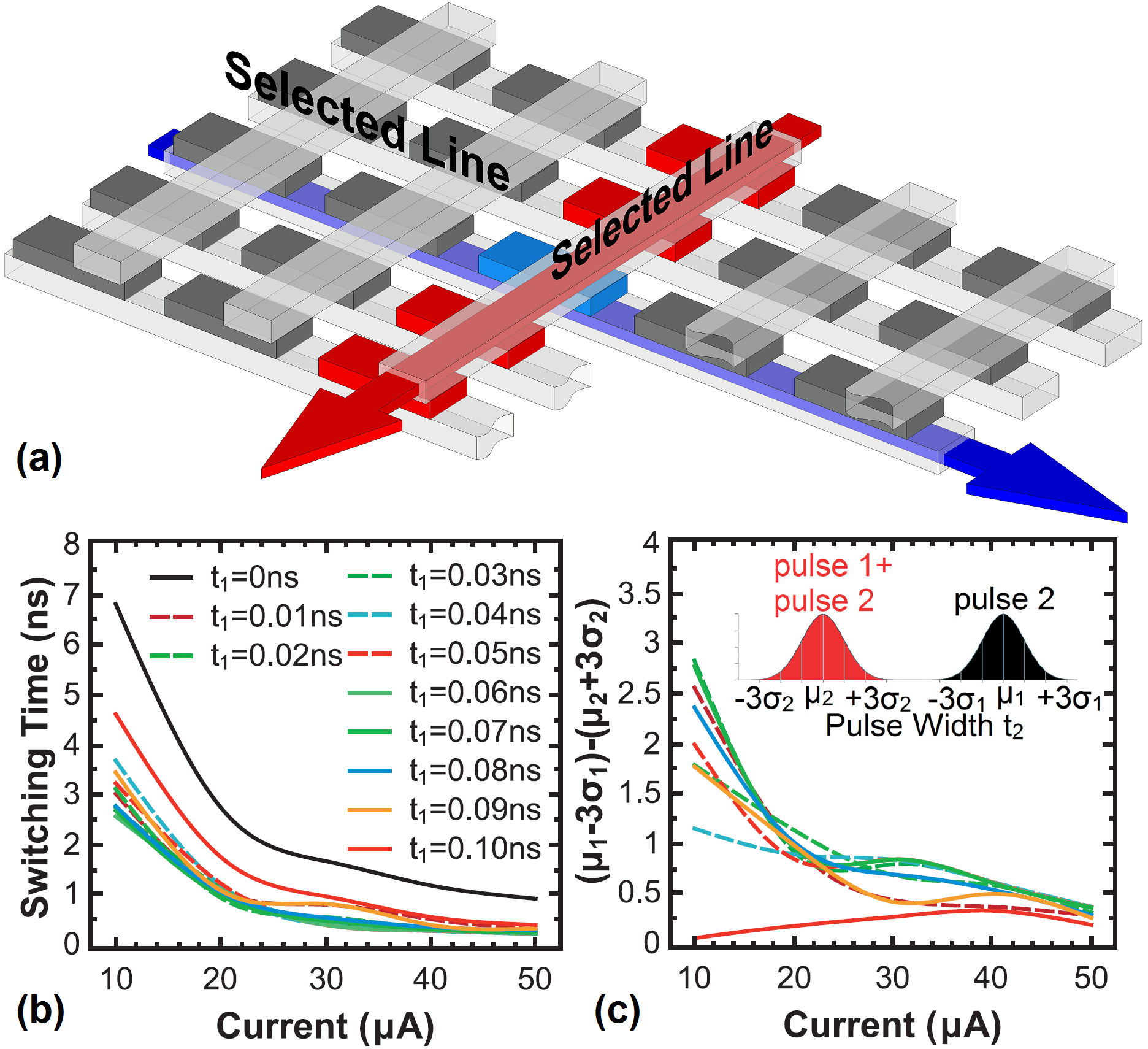
An alternative method for solving the second transistor issue is to use a cross-point architecture. The write operation in such an architecture is based on two consecutive orthogonal sub-nanosecond in-plane current pulses (Fig. 1a). In contrast to conventional SOT-MRAM, this architecture does not require an external magnetic field.
We investigated an SOT-MRAM based on cross-point architecture by means of extensive micromagnetic simulations. Our simulations reveal that increasing the current value to 40 μA accelerates the switching beyond half a nanosecond (Fig. 1b). We also demonstrated the absence of switching in cases where only one of the two pulses is used (Fig. 1c).

Fig. 1: (a) Schematic illustration of a cross-point architecture for the switching of the soft magnetic layer by means of consecutive orthogonal sub-nanosecond current pulses. The blue and red arrows indicate "write pulse 1" and "write pulse 2", respectively. (b) Switching time as a function of current. (c) The difference between the minimum value of the pulse width t2, which is required to achieve a non-zero probability of switching by using the "write pulse 2" (μ1-3σ1), and the value of the pulse width t2 needed to achieve guaranteed switching with the "two write pulses" (μ2+3σ2) as a function of current.


