 |
|
Biography
Marco Rovitto was born in Milan, Italy, in 1985. He studied material science at the Università degli Studi di Milano-Bicocca, where he received the bachelor's degree in 2010 and the master's degree in 2013. He joined the Institute for Microelectronics in January 2014, where he is currently working on his doctoral degree. His scientific interests include electromigration, interconnects, and process simulations.
Electromigration Reliability Issues in Interconnects for Three-Dimensional Integration Technologies
Innovation in the semiconductor industry has enabled transistor scaling along Moore's law for many decades. More recently, significant effort has been dedicated to the introduction of diversified functionality on a single chip. Attempts to realize this on a single plane result in interconnect congestion, as well as increased circuit noise and delay.
These issues could be overcome by vertically stacking multiple technologies located on different planes of the chip and by providing electrical interconnection by making use of the third dimension. Although interconnect technologies for three-dimensional integration show significant advantages, there are several reliability concerns, as is often the case in emerging technologies.
A key reliability issue in modern conducting structures is the influence of electromigration, which is the process of mass-transport-induced failure caused by high current flow in metal lines, on device lifetimes. The prediction of the electromigration lifetime becomes crucial for the assessment of interconnect reliability. Accelerated electromigration testing has been used for decades to determine the factors affecting the lifetime of interconnects, but the mechanisms governing failure are extremely difficult to identify. The most feasible way is to use physical modeling.
In general, electromigration modeling presents a multiphysics problem, which can be divided into two phases, namely, the early phase of void nucleation and the late phase of void evolution. During the first phase, stable voids nucleate in the interconnect due to the development of tensile stress, particularly at those locations where the adhesion between the metal layer and the surrounding material is weak. In turn, the late phase is governed by the void evolution mechanism, which leads to extremely high changes in interconnect resistance until open-circuit failure is noted.
The lifetime of the interconnect can be determined after reaching the maximum tolerable resistance value in the given circuit. By implementing this two-phase model in a commercial software, based on the finite element method, one can carry out numerical simulations in an efficient way.
Electromigration simulations were performed for realistic interconnect geometries in order to assess their reliability. A number of case studies were undertaken concerning through-silicon vias (TSVs) and flip-chip solder bumps.
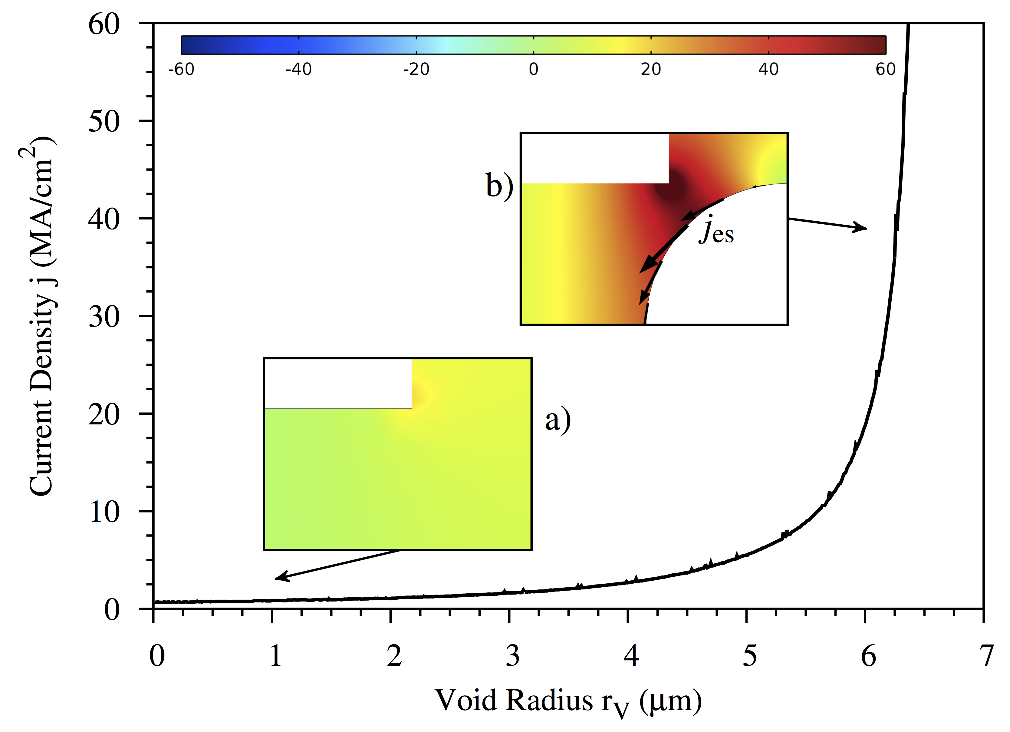
In the first study, electromigration failure was seen to originate close to the metallization barrier between the via and the adjacent metal layer. Once the void nucleated, its growth was fueled by the electromigration-induced-vacancy flux along the void surface (Fig. 1). The combination of the kinetics of both phases of failure was found to provide a good estimate of interconnect lifetime.
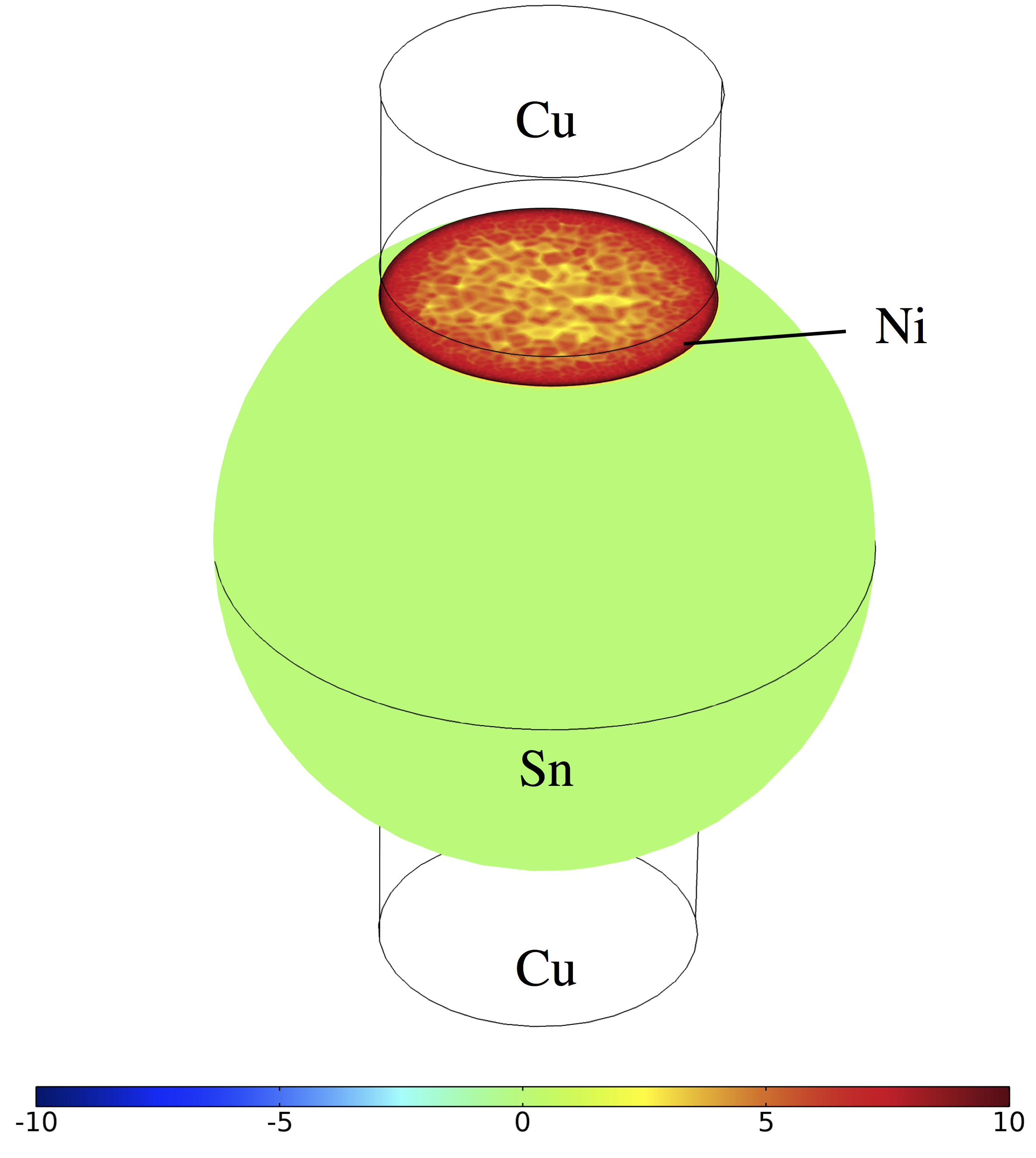
In flip-chip solder bump technologies, electromigration enhances changes that occur in the material composition, which leads to void nucleation at the bump/under bump metallization (UBM) interface (Fig. 2). These analyses showed that the solder bump lifetime is dominated by the early failure phase. Furthermore, it was found that simulations are capable of reproducing the electromigration phenomenon in diverse structures and of producing meaningful results for the purposes of reliability evaluation.

Fig. 1: Current density dependence on the void radius in an open copper TSV. Cross-section views of the current density distribution are shown at two different void radii rv: a) 10 nm and b) 6 ?m. The distribution of the average current density over the void surface is represented by the arrows.

Fig. 2: Profile view of the mechanical stress distribution in the solder bump geometry after fourteen hours of current flow. The maximum tensile stress is located at the top of the Sn bump beneath the Ni UBM layer.


