 |
|
Biography
Gerhard Rzepa received the BSc degree in Electrical Engineering in 2010 and the Diplomingenieur degree in Microelectronics in 2013, both from the TU Wien (Vienna University of Technology). Since 2013 he is working on his doctoral degree at the Institute for Microelectronics, TU Wien. His main research interests are oxide degradation, device variability and measuring and modeling of related reliability phenomena such as bias temperature instabilities, hot carrier degradation, random telegraph noise, and stress induced leakage currents.
Reliable BTI Life-Time Extrapolation with an Effective Oxide Defect Model
Recent advances in physical oxide defect models based on the non-radiative multi-phonon (NMP) theory have enabled a detailed understanding of related reliability phenomena, such as bias temperature instabilities (BTI) for negative and positive (PBTI) stress, random telegraph noise and stress-induced leakage currents. An extension of the four-state NMP model, which considers hydrogen-related defect activation, also allows for understanding and modeling the peculiarities of degradation at high temperatures for long stress times.
However, these very detailed models are inherently complex and computationally expensive. This limits their practical application for lifetime predictions, which is typically done under simple biasing schemes using simple and fast power-law extrapolations. While these extrapolation methods are convenient, they lack a physical foundation and cannot be used for explorative studies of novel technologies. Furthermore, deviations from power-law characteristics are observed for experiments with large measurement times, which indicate errors in the prediction of lifetimes when this approach is used.
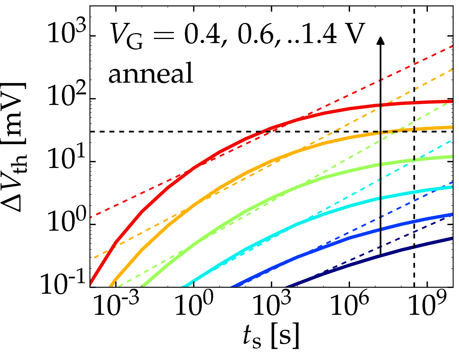
We have demonstrated that the essential features of physical defect models can be captured by a single effective NMP transition between two charge states. This model only requires simple device electrostatics, allowing for convenient and fast computations without TCAD simulations. Lifetime predictions with this model feature a saturation of the degradation after long stress times, which is observed for very long measurement times. In contrast, power-law extrapolations do not account for this saturation and therefore offer more pessimistic lifetime predictions, as shown in Fig. 1 for PBTI stress on a high-k technology.
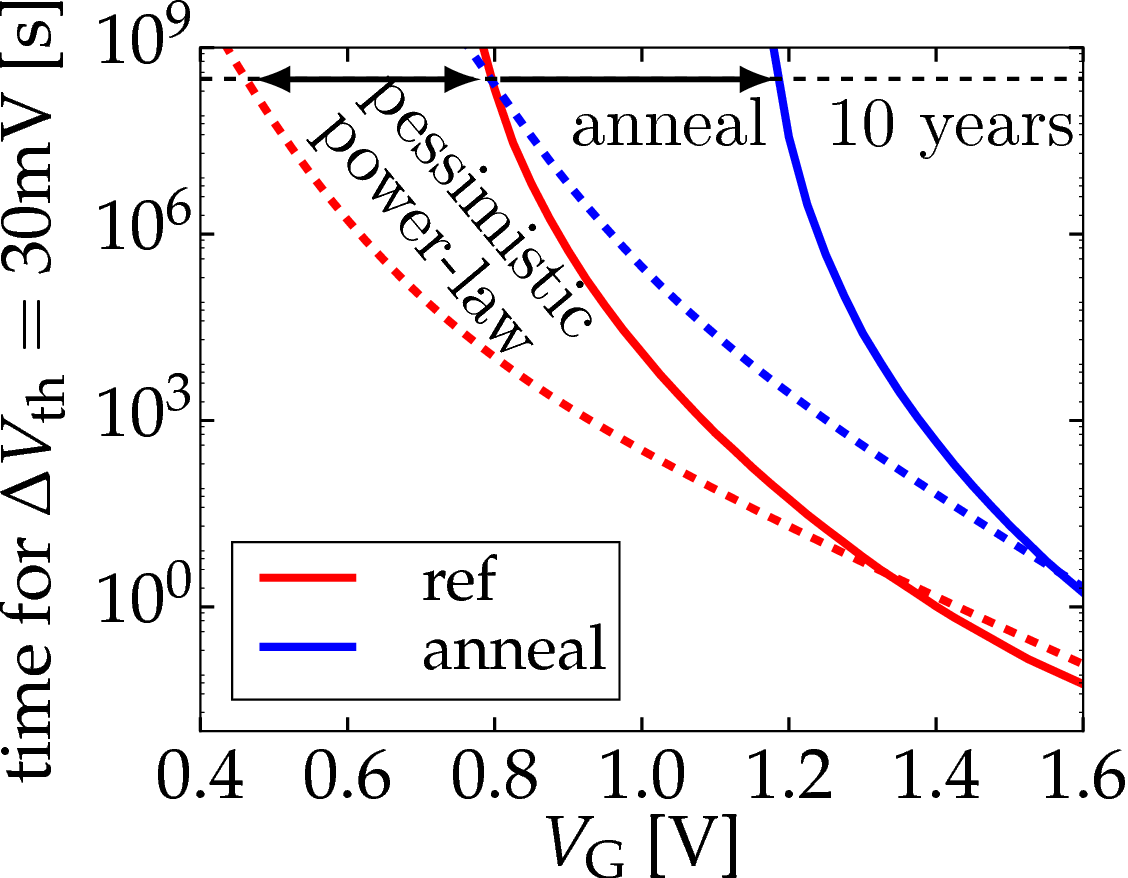
Furthermore, the impact of processing on oxides can be conveniently investigated using the physical parameters of the effective two-state NMP model. This was done for PBTI on high-k gate stacks where the impact of a post-metal anneal on the oxide was analyzed. The improvement due to this reliability anneal is shown in Fig. 2 and was found to be predominately due to a shift in the trap energy levels closer to the conduction band edges.

Fig. 1: Simulation of the PBTI threshold voltage shift (ΔVth) of a transistor at room temperature modeled using the effective two-state NMP model (solid lines) and power-law predictions based on extrapolation within the typical measurement window with stress times (tr) between 1 s and 1 ks.

Fig. 2: PBTI lifetime with a 30 mV ΔVth criterion as a function of the operating voltage VG for reference devices (red) and a device with a reliability anneal (blue) at room temperature. The extrapolation with a power-law (dashed lines) gives a much more pessimistic prediction compared to simulations with the effective two-state NMP model (solid lines).


