 |
|
Biography
Bernhard Stampfer, born in 1989 in Austria, studied at the Technische Universität Wien where he received the BSc degree in Electrical Engineering (2013) and the Diplomingenieur degree in Microelectronics and Photonics (2016). He joined the Institute for Microelectronics in March 2016, where he is working on his doctoral degree.
Random Telegraph Noise Characterization of Defects in MOS Transistors
With the continued shrinking of MOS transistors, not only has their performance increased, in terms of power consumption or switching frequency, for example, but so has their susceptibility to microscopic variations between individual devices. In current devices, even small numbers of such defects, created during fabrication or usage, might lead to premature failure of the device depending on the operating conditions. Knowledge of the defects responsible is therefore required to predict reliability and define a safe operating range to match lifetime expectations.
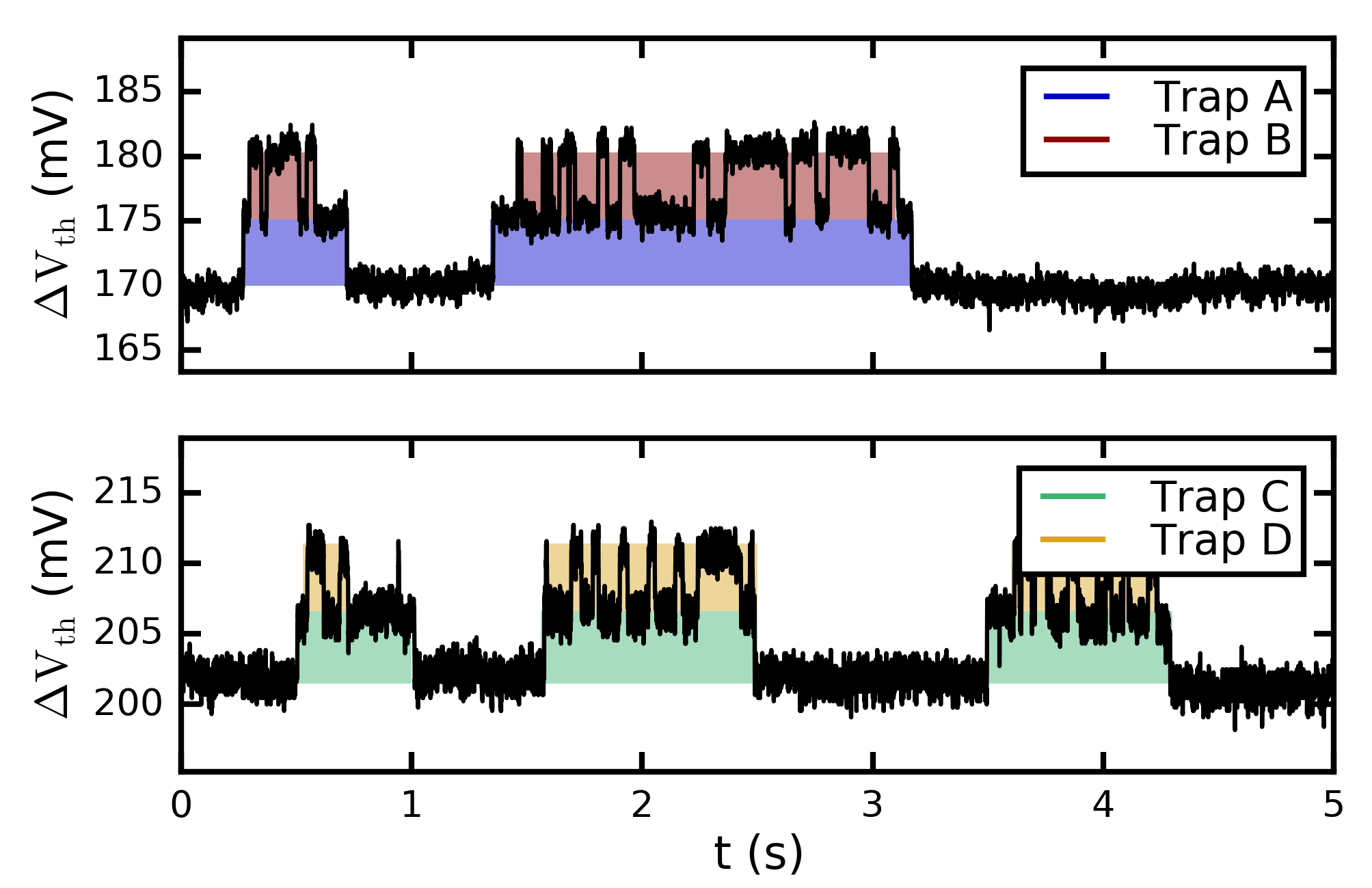
Random telegraph noise (RTN) is the temporal variation of the output current of a MOS transistor under static operating conditions caused by the individual and stochastic capture or emission of electrons by atomistic defects in the device. The charges at these defect sites influence the electric field at the conducting channel in the device, thereby leading to a change in current. In larger devices, this phenomenon is visible as an increase in noise level. In smaller devices, however, as the influence of single defects on the current grows, discrete features can be seen (Fig. 1).
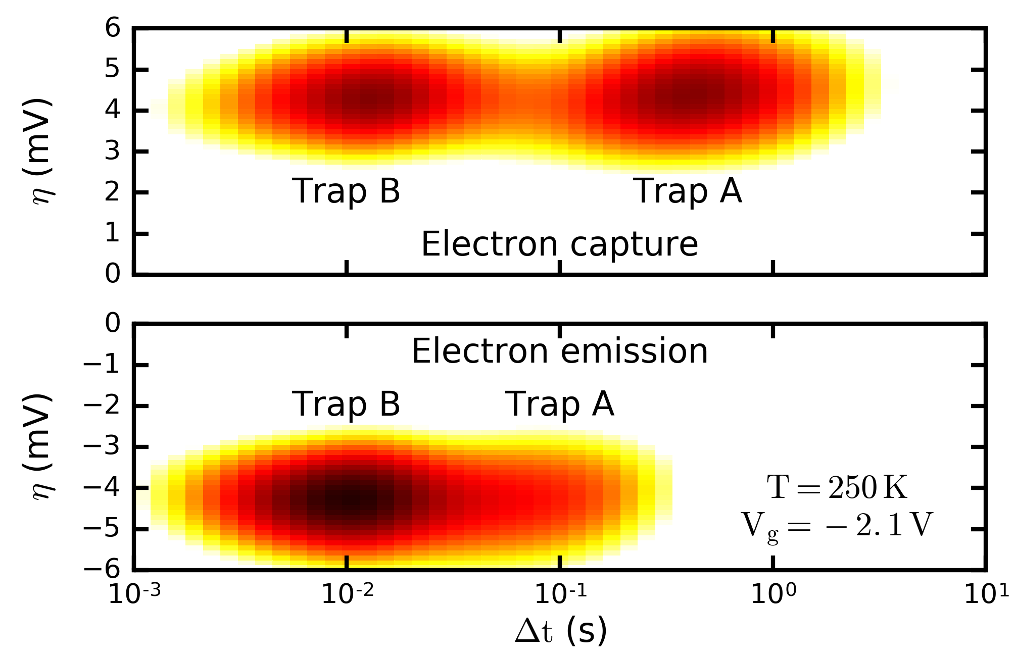
By analyzing the RTN current using statistical methods, the steps can be assigned to individual defects (Fig. 2). This analysis yields the defects' properties: step heights, capture and emission times, and possible correlations between the defects. Effort has to be expended in order for a given extraction method to be tolerant to noise, which may arise either from the measurement setup itself or from defects that are not resolvable as steps in the measurement window. This must be done while keeping the need for manual input low in order to allow for the extraction of a large number of defects. By taking measurements at varying temperatures and gate voltages, and in conjunction with stress-recovery measurements that allow a similar extraction of capture and emission times in different gate bias ranges, physical parameters of the defects, such as spatial and energetic position, as well as energy barriers, can be estimated by calculation or through comparison with device simulation. Determining the distributions of these physical properties is a crucial step towards identifying the atomistic nature of the defects responsible for reliability limitations.

Fig. 1: Discrete steps in the source current of a GaN MOSFET, mapped to an equivalent threshold voltage shift. Events A-B and C-D in this device are correlated, indicating either defects in close proximity or defects with three charge states.

Fig. 2: Distribution of capture and emission events over step height and time since the last matching emission or capture event. While similar in height, the steps can be separated by their capture and emission time distributions.


