 |
|
Biography
Bianka Ullmann was born in Sofia, Bulgaria, in 1984 and has been in living in Vienna since 1991. She received the degree of Diplomingeneur in physics from the Technische Universität Wien in 2012. She has been working as a project assistant at the Technische Universität Wien since 2013 and joined the Institute for Microelectronics in January 2014.
How Mixed Stress Conditions Affect Single Oxide Defects in MOSFETs
The international roadmap for semiconductors lists bias temperature instability (BTI) and hot-carrier degradation (HCD) as the most difficult challenges to be properly understood and modeled. Although extensive experimental and theoretical studies of these phenomena have been performed, there are still open issues in understanding the nature and behavior of material defects contributing to BTI and HCD. Furthermore, in circuits, transistors are rarely subjected to idealized BTI or HC conditions. We therefore focused on the impact of mixed negative BTI (NBTI) and HC stress on material defects in pMOSFETs. In order to characterize recoverable device degradation, we recorded the behavior of oxide defects at mixed stress conditions.
Degradation mechanisms are caused by material defects in the amorphous gate oxide of a MOSFET. These defects can capture or emit charge carriers from the substrate and from the gate oxide. The capture and emission events cause a change in the current between gate and source at constant gate-source voltage and drain-source voltage. This electrical response corresponds to an unwanted shift in device characteristics, for example, the threshold voltage. Measurements of this detrimental shift allow us to characterize the impact of different stress conditions on the device characteristics and, in the case of nanoscale MOSFETs, to observe the nature of individual defects responsible for the unwanted shifts.
Time-dependent defect spectroscopy measurements show that fewer defects contribute to the overall threshold voltage shift after mixed NBTI/HC stress than after pure NBTI stress. Although the electrostatic conditions at the source side hardly change for different stress modes at a fixed gate voltage, source-side defects can show a completely different behavior after mixed NBTI/HC stress. This observation can be explained when one considers that defect parameters can shift significantly at mixed stress conditions due to non-equilibrium processes. This occurs for all lateral positions and leads, for example, to a change in their capture and emission times.
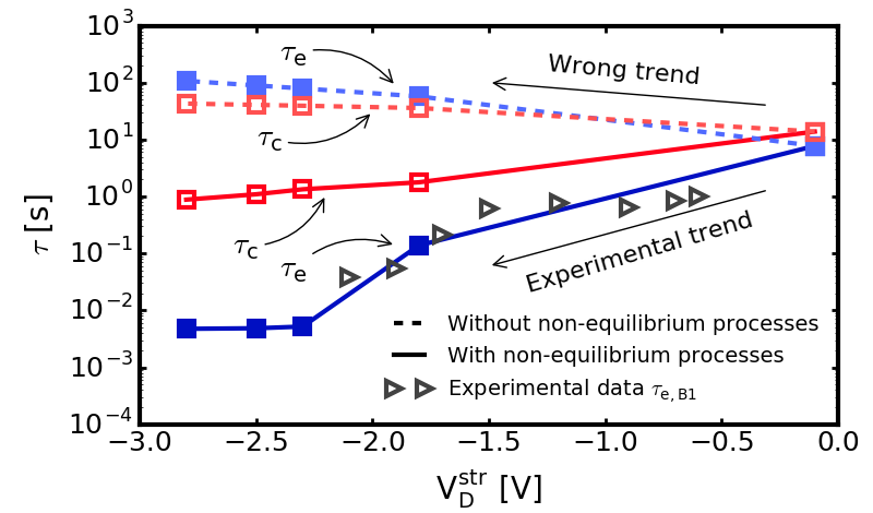
As a consequence, even if a defect captures a charge carrier during stress, it emits it immediately and thus remains neutral after stressing. Non-equilibrium processes must therefore be taken into account in existing defect models. By way of example, Fig. 2 illustrates that by modeling the capture and emission times of defect B1 at a relative lateral position of 0.71 (where 1 is at drain) by considering non-equilibrium processes, the experimental data can be explained quite well. Conversely, if defect B1 is modeled with a simple electrostatic model, the wrong trend is obtained.
In conclusion, our results suggest that non-equilibrium processes have to be taken into account in order to explain the behavior of defects responsible for the detrimental shifts of MOSFET parameters under mixed stress conditions. These results provide insight into degradation processes in a more detailed way, which is a step towards realistic MOSFET lifetime predictions under circuit operation.

Fig. 1: Comparison of modeled and measured capture and emission times. Dashed lines: Capture and emission times modeled using the non-radiative multiphonon model, assuming equilibrium carriers in the channel, which show an increasing trend simply due to the change in the oxide field. Solid lines: Capture and emission times modeled considering non-equilibrium conditions by taking into account impact ionization during the solution of Boltzmann's transport equation, which results in agreement with experimental data.


