 |
|
Biography
Michael Waltl was born in Oberndorf near Salzburg, Austria. He received the BSc degree in electrical engineering and the degree of Diplomingenieur in microelectronics from the Technische Universität Wien in 2009 and 2011, respectively. He joined the Institute for Microelectronics in January 2012, where he is currently working on his doctoral degree. His scientific interests include negative and positive bias temperature instabilities and electric measurement methods.
Advanced Measurement Setup for Single-Defect Spectroscopy
The time-to-failure of modern semiconductor devices is seriously
affected by reliability issues, such as bias temperature instabilities
(BTI) and hot carrier degradation (HCD). Both mechanisms are caused by
the creation, charging and discharging of interface states and
structural defects in the dielectric and both limit device
performance. In particular, BTI and HCD degrade the threshold voltage
of the transistor.
In most reports, measurements are performed on large area devices,
where the impact of single defects is typically obscured by
measurement noise. By probing nanoscale transistors, however, single
charge capture and emission events can be studied at a great level of
detail. During the course of performing single defect investigations
using general-purpose instruments, several limitations in available
instruments have been observed. For instance, many such setups involve
cumbersome combinations of several different instruments with partly
custom-made circuits and can produce, for instance, undocumented
delays when the bias is swept from negative to positive voltages.
We also observed that setups combining various general-purpose
instruments do not provide the long-term measurement stability
required for monitoring permanent threshold voltage drifts over
several months. To circumvent these limitations, we have been
developing our own measurement instrument, called the time-dependent
defect spectroscopy measurement instrument (TMI). The TMI combines
voltage units, which allow to create arbitrary and highly accurate
programmable voltage signals, as well as data sampling units to
monitor currents in the sub-picoampere regime. Furthermore, the TMI
supports a high sampling frequency, currently up to 1 MHz, even in the
picoampere regime. Another significant advantage of the TMI is that it
offers up to sixteen programmable digital inputs and outputs. These
can be used to either synchronize the TMI with general-purpose
instruments or to trigger device selection, for instance for
transistors arranged in dedicated array structures.
Using the TMI, charge trapping by single defects in conventional SiO2
n-channel and p-channel transistors has been monitored, as well as in
transistors employing high-k dielectrics and in exotic two-dimensional
devices. Quite recently, the TMI was used to probe single defects in a
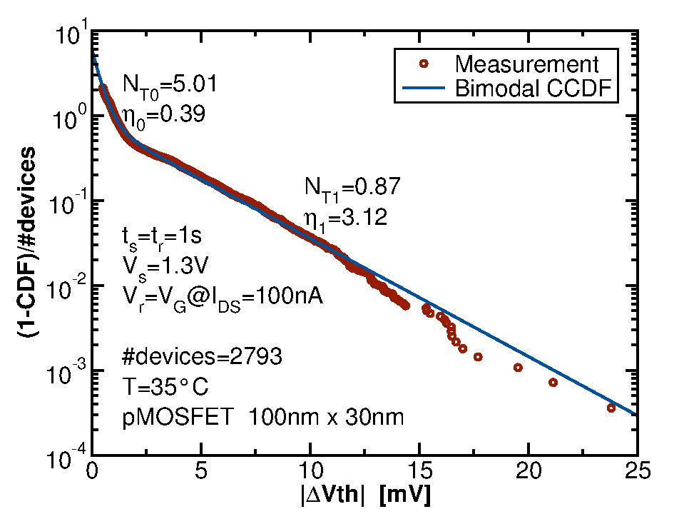
52k transistor array structure. In this application, the drift of the
threshold voltage for around three thousand p-channel, high-k
transistors was automatically recorded and analyzed. As shown in
Fig. 1, bimodally distributed step heights of the single charge
emission events were found.
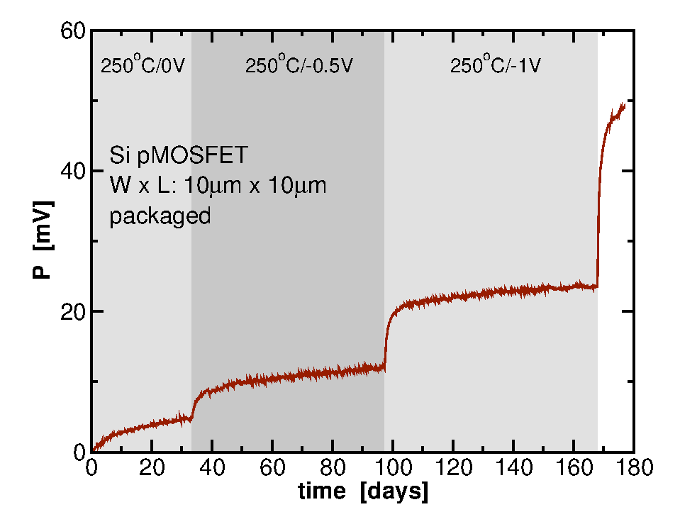
Another important application of the TMI is the characterization of
the permanent degradation of BTI. As charge transition times of the
single defects contributing to a permanent shift in threshold voltage
typically exceed several days, weeks or even months, long-term stable
measurements have to be performed. With the TMI, measurement times as
long as nine months have been performed without any interruption (see
Fig. 2).
Overall, the TMI is a powerful measurement instrument, which offers
many features necessary for the successful characterization of device
degradation mechanisms. Due to its modular design, the TMI can be
individually adjusted to experimental requirements.

Fig. 1: A bimodal cumulative complementary distribution function of step heights is extracted from a very large number of p-channel transistors.

Fig. 2: Longtime measurements can be performed without any interruption. Quite remarkably, a permanent drift in the threshold voltage is already built up even at zero gate bias. Note that the experiments are performed at a high temperature, which accelerates the accumulation of P.


