 |
|
Biography
Milica Gadjanski was born in Zrenjanin, Serbia, in 1978. She studied mechanical engineering, department of the aerospace engineering, at the Technical University of Belgrade, Serbia, where she received her Master (Dipl.-Ing.) degree in 2008. After working many years in automotive industry, by invitation, she came at TU Wien for doctoral research study. From 2013 to 2017 Milica was working as a scientific assistant at the Institute for Powertrains and Automotive Technology (TU Wien) in the field of fuel cell vehicles, where she finished her doctorate in February 2017. She joined the Institute for Microelectronics in May 2017 as a postdoctoral researcher, focusing on simulation on mechanical effects as part of the SOITEC SmartCut process.
The Haasen-Alexander-Sumino Model and the Thermo-Mechanical Deformation of Silicon Wafers
Investigations that lead to a better understanding of the plastic deformation of silicon wafers during thermal processing are of major interest in microelectronics. Such investigations aim to help predict plastic wafer warping and to facilitate its reduction to an acceptable level. The plastic deformation of silicon wafers is comprehensively described by the Haasen-Alexander-Sumino (HAS) model, which relates time-dependent creep strain to the dislocation density distribution inside the silicon wafer. The model itself includes phenomenological relations that describe dislocation migration and multiplication. The HAS model is a combination of the Orowan model (plastic strain, dislocation velocity), the Alexander-Haasen model (dislocation velocity, dislocation interactions) and the Johnson-Gilman model (dislocation population dynamics). One of the model's main limitations is the fact that its predictions strongly depend on the initial dislocation distribution, which is generally unknown. To obtain a realistic picture of the initial dislocation distribution, a careful study of the crystal growth process is needed.
The mathematical description of the HAS model consists of a system of partial differential equations, which need to be solved simultaneously with an accompanying conductive heat transfer model and linear thermoelastic model. For the practical implementation of the HAS, as well as the aforementioned accompanying models, the software Multiphysics® program was used for the purposes of conducting simulation studies. Simulative studies include different analytical initial dislocation densities, different temperature profiles, and different shapes and positions of wafer supporting nodes. The goal of the research is to find initial and boundary conditions that would reduce wafer deformation to a minimum. Fig. 1 shows the displacement field in the z-direction of an Si wafer after thermal processing. The wafer deformation is triggered by gravity and the inhomogeneity of the temperature distribution during the heating and cooling processes. The result is a shear stress at the top of the wafer and a tensile stress at its bottom.
Future work will consider extending the original HAS model to include multiple slip systems, the immobilization of mobile dislocations, jog formation between different slip systems, and its influence on dislocation generation and internal stress due to short-range interactions from the total dislocation density.
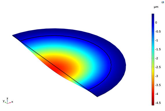
Fig. 1: The displacement field z-component in micrometers of a silicon wafer after the thermal process with a constant initial distribution of dislocations.