 |
|
Biography
Yury Illarionov was born in Leningrad (now Saint-Petersburg) in 1988. He studied solid state physics at the Physical Science and Technology Faculty of St. Petersburg State Polytechnical University where he received the B.Sc. and M.Sc. degrees in 2009 and 2011, respectively. From 2010 to 2012 he studied advanced material science in Grenoble Institute of Technology (France) and University of Augsburg (Germany) in frameworks of Functionalized Advanced Materials and Engineering (FAME) Erasmus Mundus program and in September 2012 received a double European M.Sc. degree. His scientific carrier has started in October 2007 in Ioffe Physical-Technical Institute (Russia) and in November 2011 he joined the PhD program there. He also visited IRCELYON (France, May-July 2011) and Singapore Institute of Manufacturing Technology (Singapore, February-July 2012) as a young guest researcher. He joined the Institute for Microelectronics in February 2013. In January 2015 he received the PhD degree in semiconductor physics from Ioffe Physical-Technical Institute and in December 2015 the Dr.techn. degree from Technische Universität Wien. Since January 2016 Dr. Yury Illarionov is a postdoc researcher working on reliability of the next-generation 2D FETs with graphene, MoS2 and phosphorene.
Single-Layer MoS2 Field-Effect Transistors with 109 On/Off Current Ratios and Improved Reliability
Molybdenum disulfide (MoS2) is a promising “beyond graphene” material that is now being considered for application in next-generation 2D electronics. Recently, considerable progress in the fabrication of single-layer (1L) MoS2 field-effect transistors (FETs) has been demonstrated. However, the reliability of these devices is still not competitive compared to their Si counterparts. At the same time, the typical on/off current ratios of previously reported MoS2 FETs are within 105-107, which also requires further improvement. As such, fundamentally new technological steps have to be suggested to make these devices commercially competitive.
In 2017, we examined 1L back-gated MoS2 FETs (see Fig. 1a provided by Stanford University) with the high-quality MoS2 channel grown by chemical vapor deposition (CVD) directly on a SiO2(25nm)/Si substrate. In order to protect the channel from the impact of the ambient environment, the devices were encapsulated with a high-quality 15 nm thick Al2O3 layer grown by atomic layer deposition at 300°C. As shown in Fig. 1b, the on/off current ratio of these MoS2 FETs can be as high as ~109, which is higher than reported elsewhere and thus can be considered a world record for 1L semiconductors. Furthermore, the typical hysteresis widths (Fig. 1c-d) and bias-temperature instability (BTI) drifts (Fig. 1e) are up to two orders of magnitudes smaller compared to our previously studied bare exfoliated devices. As shown in Fig. 1c-d, where we also provide the results for bare CVD-grown devices, these improvements are achieved by the combined use of a CVD-grown MoS2 channel and a high-quality Al2O3 capping layer. In particular, the use of CVD-grown MoS2 likely allows for a reduction in the number of channel defects (e.g. S vacancies), and the high-quality Al2O3 layer reliably protects the channel from adsorbate-type traps, which are known to contribute to hysteresis and BTI. As such, we conclude that both the CVD growth of the MoS2 channel and the Al2O3 encapsulation represent important technological steps towards reaching commercial quality standards for the performance and reliability of next-generation MoS2 devices.
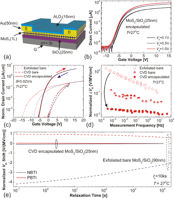
Fig. 1: (a) Schematic layout of the CVD-grown 1L MoS2 FETs, with 15 nm thick Al2O3 encapsulation (provided by Stanford University). (b) The Id-Vg characteristics of these devices show an on/off current ratio of up to 109. (c) The Id-Vg characteristics of bare exfoliated MoS2/SiO2(90 nm) FET and CVD-grown bare and encapsulated MoS2/SiO2(25 nm) devices measured using the sweep rate S = 0.02 V/s and normalized by the channel widths. (d) The hysteresis widths extracted for these three devices and normalized by the oxide field factor versus the measurement frequency, f. (e) Negative BTI and positive BTI recovery traces normalized by the oxide field for bare exfoliated and encapsulated CVD-grown MoS2 FETs.