 |
|
Biography
Hans Kosina received the Diplomingenieur degree in electrical engineering and PhD from the Technische Universität Wien in 1987 and 1992, respectively. He was with the Institute of Flexible Automation at the Technische Universität Wien for one year and then joined the Institute for Microelectronics, where he is currently an Associate Professor. He received the venia docendi in microelectronics in 1998. In the summer of 1993, he was a visiting scientist at Motorola Inc., Austin, Texas, and in the summer of 1999, a visiting scientist at Intel Corp., Santa Clara, California. Dr. Kosina served as a Technical Program Committee member in the IEEE International Workshop on Computational Electronics in 2003 and 2004 and was the chairman of the ''11th International Workshop on Computational Electronics'' held in Vienna in May 2006. He has served as the Associate Editor of the IEEE Transactions on Computer-Aided Design of Circuits and Systems since January 2004. His current research interests include the device modeling of semiconductor devices, nanoelectronic devices, organic semiconductors and optoelectronic devices, the development of novel Monte Carlo algorithms for classical and quantum transport problems, and computer-aided engineering in ULSI-technology.
Electronic Transport in Semiconductor Devices and Nanostructures
When designing new semiconductor devices and materials with features approaching the nanometer scale, the key physics governing the flow of charge changes from the classical to the quantum mechanical. Ongoing work within our group has focused on the development of numerical methods and algorithms for both classical and quantum mechanical transport calculations.
Quantum transport is most rigorously modeled using non-equilibrium Green's functions (NEGF). Our work on NEGF is being integrated into the commercially available Vienna Schroedinger-Poisson solver. This tool allows for the analysis of devices with irregular geometries and situations where transport physics is quantum mechanical but still dominated by scattering with phonons. A number of open questions concerning the application of the NEGF formalism to unstructured finite-volume meshes have been solved.
Quantum transport models less complex than NEGF can be formulated in terms of the density matrix or the Wigner function. There is a third option based on what we call the sigma function. It is intermediate between the density matrix and the Wigner function. Fourier transformation of sigma gives the Wigner function. To study the sigma equation we made a comparison with Frensley's finite-difference Wigner method. For both equations we have developed a shooting method. This method allows one to use very fine meshes and is well suited for parallelization. All operators in the sigma equation can be sparsely discretized. Simulations of a resonant tunneling diode have been performed. The sigma equation yields a numerically accurate solution, which does not noticeably change if the mesh is further refined. However, the resulting current/voltage curve is unphysically high and does not show the expected resonance peak. Frensley's discretization of the Wigner equation results in a physically meaningful current/voltage curve for a rather coarse grid (800 Nodes), but approaches the unphysical solution of the sigma equation when the grid is extremely refined (102,400 Nodes). Frensley's discretization uses upwinding for the spatial first order derivative. Upwinding on a coarse mesh introduces a considerable amount of artificial diffusion. This actually results in a very large numerical error but seems to benefit the physics, at least in this application. Future work will attempt to gain understanding of the observed breakdown of the stationary Wigner equation in the semi-discrete limit.
With respect to classical transport, we continued the development of the Vienna Monte Carlo device simulator (VMC). Various models and algorithms, which were already implemented in the full-band part of the VMC, have been implemented for analytical band structures as well. In particular, to compare the results of full-band simulations with those of analytic-band simulations, an electron-electron scattering model for analytical bands has been implemented. In some cases, an enhancement of the high-energy tail of the distribution function has been observed due to electron-electron scattering. Although in the literature it is commonly accepted that this enhancement is a physical effect and should be taken into account in the modeling of hot-carrier degradation, our analysis indicates that this enhancement could be unphysical and a mere result of the approximate treatment of the partner electrons.
Progress was also made with the backward Monte Carlo method. A current estimator based on a symmetric sampling of the k-space has been developed. It reduces the statistical error for all operating conditions of a device and becomes particularly effective at small current levels. The figure shows the acceleration integral evaluated at the surface of a 65 nm gate length MOSFET, which is a measure for the bond breaking rate during hot-carrier stress. A range of 30 orders of magnitude can be resolved using the backward method. This range would be unattainable using a forward method.
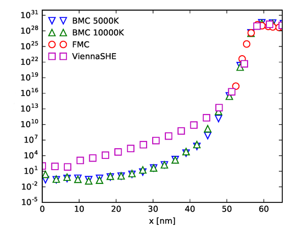
Fig. 1: Acceleration integral for a 65 nm nMOS, simulated with forward Monte Carlo and backward Monte Carlo at different injection temperatures. The result of the deterministic Boltzmann solver, ViennaSHE, is shown for comparison.