|
|
Biography
Gerhard Rzepa received a BSc degree in Electrical Engineering in 2010 and a Diplomingenieur degree in Microelectronics in 2013, both from the TU Wien (Vienna University of Technology). In 2018 he finished his PhD studies on the topic of modeling of bias temperature instabilities at the Institute for Microelectronics, TU Wien, and obtained his doctoral degree. He continues to work at the Institute for Microelectronics where he focuses on the research of oxide degradation, device variability and measuring and modeling of related reliability phenomena such as bias temperature instabilities, hot carrier degradation, random telegraph noise, and stress-induced leakage currents.
Comphy: A Compact-Physics Framework for the Unified Modeling of Bias Temperature Instabilities
In recent years, a gap has emerged between the understanding of oxide degradation, on the one hand, and the application of models in industry, on the other hand. Very detailed physical models have been developed around the non-radiative multi-phonon theory, which consider hydrogen-related defect activation in order to understand a broad range of phenomena related to bias temperature instabilities (BTI). This enables the accurate prediction of transistor characteristics under various stress conditions. However, research departments that monitor the production and development of metal-oxide-semiconductor (MOS) technologies must handle a vast amount of measurement data. They therefore need quick and convenient tools to analyze process splits.
In order to fill this gap, we have developed a simulation framework called "Comphy", short for compact-physics. This framework takes the central concepts of the detailed physical models, which are necessary to characterize BTI, in order to enable physical insights and pathfinding for future technologies with arbitrary stress signals and temperatures. Still, Comphy is designed to act as a slim and fast tool that can also be employed in standard characterization routines to compute physical properties and reliability projections within seconds.
The accuracy of Comphy was demonstrated successfully on a technology targeting the periphery of DRAM chips. Four different process splits were tested in this study, starting with a plain SiO2 oxide. In another split, an HfO2 layer was deposited on top of that, followed by a split with another thin layer of Al2O3 on top. In the fourth split, the Al2O3 layer was selectively removed. BTI data for negative (NBTI) and positive (PBTI) stress measured in pMOS and nMOS devices for these splits gave a consistent picture of the oxide defects (see Fig. 1). A very peculiar observation, in the device with the thin Al2O3 layer, was previously reported in the literature as anomalous PBTI. While regular PBTI is dominated by electron capture during stress, which causes a positive shift in the threshold voltage (ΔVth), the opposite can be observed for electron emission during stress. The simulations with Comphy inherently reproduce this phenomenon, corroborating that the physics of the governing degradation mechanisms is correctly modeled (see Fig. 2).
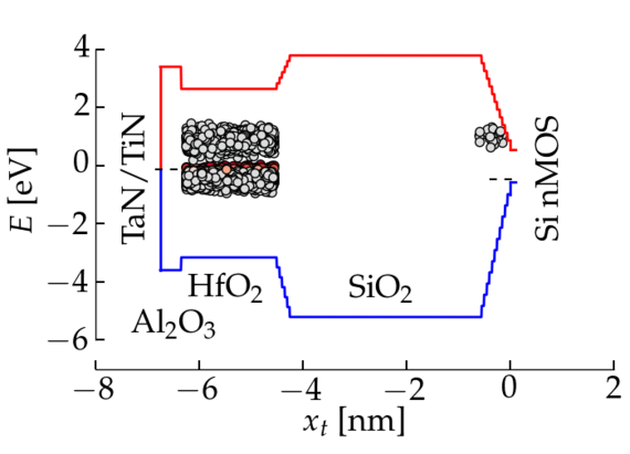
Fig. 1: The band diagram of an nMOS transistor with a thin layer of Al2O3 on top of HfO2 and SiO2. Depicted are the defects (circles: red for positive, gray for neutral) that can contribute at PBTI conditions.
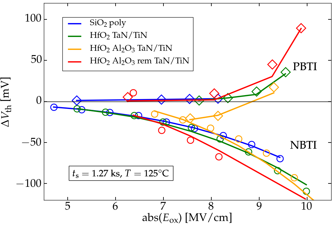
Fig. 2: Measured degradation after 1.27 ks of PBTI (diamonds) and NBTI (circles) stress at 125℃ for various oxide fields (Eox). Anomalous PBTI is apparent as a negative shift of ΔVth at positive stress voltages. Only at very large positive stress voltages, is regular PBTI degradation observed. Comphy simulations (lines) reproduce all features with a consistent set of defects across all four technologies.