 |
|
Biography
Bernhard Stampfer, born in 1989 in Austria, studied at the Technische Universität Wien where he received the BSc degree in Electrical Engineering (2013) and the Diplomingenieur degree in Microelectronics and Photonics (2016). He joined the Institute for Microelectronics in March 2016, where he is working on his doctoral degree.
Characterization of Single Defects in MoS2 Field-Effect Transistors
Transistors based on MoS2 have received a lot of attention recently, partly due to their large band gap compared to other 2D materials. Compared to mature technologies, however, MoS2 devices are still heavily influenced by defects in the material stack, which cause hysteresis, degraded mobility and long-term drift. Knowledge of the nature of these defects could improve the design and quality of MoS2 devices, as well as our understanding of other 2D materials.
By measuring an effect called random telegraph noise (RTN), we characterized individual defects in MoS2 devices. RTN is the temporal variation of the output current of a MOS transistor at static operating conditions, caused by the individual and stochastic capture or emission of electrons by point defects in the device. The charges at these defect sites influence the electric field at the conducting channel in the device leading to a change in current. In bigger devices, this phenomenon is visible as an increase in low-frequency noise level. In smaller devices, however, as the influence of single defects on the current grows, discrete steps become observable (Fig. 1).
By analyzing the RTN steps using hidden Markov models, the steps can be assigned to individual defects. This analysis offers insight into the properties of the defects: Step heights, capture and emission times, and possible correlations between the defects. From the dependence of the capture and emission time constants on gate bias and temperature, physical parameters of different defects, such as the spatial and energetic positions, can be extracted using either estimation formulas or numerical device simulations (Fig. 2). As can be seen from the Fig. 2, this allows us to distinguish between whether the defect is in the oxide or on top of the MoS2 channel, either as an adsorbate or as an intrinsic defect in the MoS2.
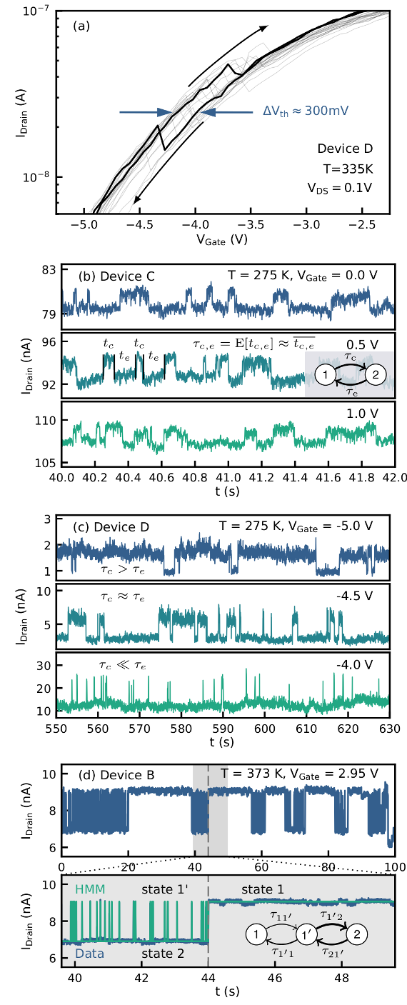
Fig. 1: Effect of defects in the devices: (a) Charging and discharging of a defect causes a shift in the ID-VG characteristics of the device; (b) two-state RTN of the drain current and its dependence on the gate bias; (c) two-state RTN of a bias independent defect; and (d) RTN caused by a three-state defect.
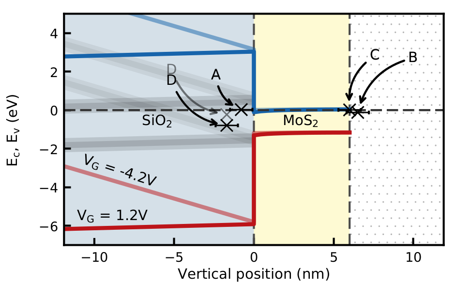
Fig. 2: Positions of the extracted defects in the gate stack of the devices.