With regard to the tunneling path, two approaches have been investigated and implemented in MINIMOS [160]:
 .
For direct tunneling, is the direct band gap (at
.
For direct tunneling, is the direct band gap (at
 ). In phonon-assisted tunneling,
 for the phonon
absorption and
for the phonon
absorption and  for
the phonon emission, where
for
the phonon emission, where  is the phonon energy and
 is the silicon band gap.
The tunneling path found in this way is perpendicular to the corresponding
equipotential lines assuming sufficiently fine local grid. Since the
tunneling length
is the silicon band gap.
The tunneling path found in this way is perpendicular to the corresponding
equipotential lines assuming sufficiently fine local grid. Since the
tunneling length  is shorter than the curvature of the equipotential
lines in common cases, tunneling between the starting point and the
endpoint may be treated like a planar one-dimensional problem. These
conditions are schematically shown in Figure 4.2.
is shorter than the curvature of the equipotential
lines in common cases, tunneling between the starting point and the
endpoint may be treated like a planar one-dimensional problem. These
conditions are schematically shown in Figure 4.2.
 which is associated with an
individual tunneling path, the models for direct and indirect tunneling as
function of the electric field at the starting point
which is associated with an
individual tunneling path, the models for direct and indirect tunneling as
function of the electric field at the starting point  , an average field
along the tunneling path
, an average field
along the tunneling path  and the field
variable from to the field at the endpoint
and the field
variable from to the field at the endpoint  have been considered.
We have assumed that the electric field strength linearly varies along the
tunneling path [456][229][170]:
have been considered.
We have assumed that the electric field strength linearly varies along the
tunneling path [456][229][170]:
 . This assumption is correct for the
totally-depleted region in one dimension. Our analysis show, however, that the
linear field variation can only be considered as an approximation for the
gate/drain overlap region. In Appendix H, an approximate model
for direct tunneling in a linearly variable field
. This assumption is correct for the
totally-depleted region in one dimension. Our analysis show, however, that the
linear field variation can only be considered as an approximation for the
gate/drain overlap region. In Appendix H, an approximate model
for direct tunneling in a linearly variable field  is derived. The
model reduces to Kane-Keldysh expression
is derived. The
model reduces to Kane-Keldysh expression  in a constant
field [244][237][236], including the dependence of the transition
probability on the transverse impulse component
in a constant
field [244][237][236], including the dependence of the transition
probability on the transverse impulse component  . The
expressions
. The
expressions  ,
,  and
and  are employed
in both, the one-dimensional and the two-dimensional approach and compared with
each other in the following section. Note that direct tunneling models are
assumed in the comparison although the MOSFETs of interest are silicon devices.
The reason for that is the present lack of expressions for phonon-assisted
tunneling in a variable field.
are employed
in both, the one-dimensional and the two-dimensional approach and compared with
each other in the following section. Note that direct tunneling models are
assumed in the comparison although the MOSFETs of interest are silicon devices.
The reason for that is the present lack of expressions for phonon-assisted
tunneling in a variable field.
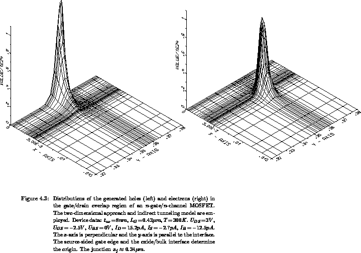
The calculated generation rates of electrons and holes are separated in the
position space, as can be seen in Figure 4.3. The proper spatial
positions of the generated carriers could be of importance when the secondary
effects are analyzed, like the acceleration of the generated carriers and
thereby induced impact ionization and hot-carrier injection. Note that the
local electric field strength can differ significantly at the places where the
holes and electrons are generated ( versus ). The generation rates
are coupled with the continuity equations via the generation terms in a
selfconsistent manner after filtering. The total charge in devices is strictly
conserved. The filtering is only applied for smoothing the distributions of the
generated carriers, to allow an efficient and automatic grid adaption in the
critical areas. Since the tunneling rate is strongly dependent on the electric
field, tunneling analysis is done on the grid which is finer than the mesh
for solving the basic semiconductor equations.
Terminal currents are calculated by an accurate technique which is derived assuming the local concentration-dependent weighting functions, as noted in Section 3.2.4.