The Potential and Field Distributions in the Critical Area


Next: 5 Summary
Up: 4.2 Numerical Analysis of
Previous: Two-Dimensional Numerical Approach
The amount and the distributions of the carriers generated by tunneling are
investigated at different gate, drain and bulk voltages, assuming graded (doped
by P) and abrupt (doped by As) drain junctions. The junctions are single
implanted. The resulting distributions of the generated electrons and holes
for a graded drain junction are presented in Figures 4.4 and
for an abrupt junction in Figures 4.5. In all four bias
conditions the gate-drain voltage is hold constant at  , while the
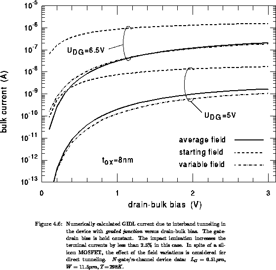
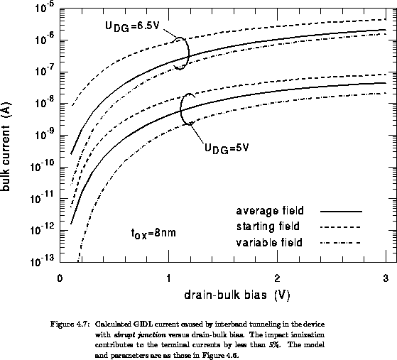
drain-bulk bias is varied. The complete characteristics, i.e. the leakage
current versus the drain-bulk bias with a constant gate-drain bias as a
parameter, for these junctions are shown in Figures 4.6
and 4.7. These characteristics nicely reflect the
two-dimensional nature of the potential distribution in the critical area.
Although the quantitative conclusions are different for every specific
technology, some general observations can be made:
- The one-dimensional (1D) approach to find the tunneling path yields
significantly lower generation rates compared to the two-dimensional (2D)
model, because the endpoints are found to lie much deeper in the bulk.
The claim holds for both, graded and abrupt junctions;
Figures 4.4 (a and b) and 4.5 (a and b).
The tunneling current, occurring as
 and
and  , is smaller in the
1D than in the 2D model for the following two reasons:
(1) The area where tunneling occurs is a bit larger in the 2D
approach than in the 1D approach due to tunneling in the lateral
direction. Therefore, even if the tunneling rate is assumed to be
dependent on the initial field  , the current
  is smaller
in the 1D than in the 2D approach.
(2) The average  is much layer in the 1D model. If we assume a
 model or a variable field
  model, the
 becomes much smaller in the 1D approach in comparison with the
2D method. Consequently, the 1D approach to find the tunneling path
cannot be applied due to a strongly two-dimensional distribution of
the potential and the field in the gate/drain overlap
region [347][326][260][189][170][73][4].
- Let us focus on the case with the P-doped junction shown in
Figures 4.4. Assuming a constant
 , the field
distribution in the critical area close to the interface
 changes weakly with
  . The magnitude of the
surface field is only determined by
  , because the lateral
component of the field is small compared to the component perpendicular
to the interface (graded junction). Deeper in the bulk (about
  ),
where the transverse field component is significantly reduced, the field
strength changes as a function of
  as well, due to the lateral
field which is no more negligible in comparison with the transverse field
component. Therefore, the field
  at the starting points which are
located close to the interface, depends strongly on
  , but weakly
on
  , while the endfield
  increases with increasing
  .
These findings enable us to explain the roll-off of the tunneling
current with decreasing
  at a constant
  , obtained
experimentally in [347] and found in our calculations as well,
Figure 4.6. At
  , equilibrium holds in
the bulk and tunneling vanishes. When
  increases, the
band-bending which is necessary for tunneling occurs already at a low
drain-bulk bias, Figure 4.4(d). However, if we assume
 for the generation model, the total tunneling current
is still small, although
  is very large due to a large
  . By
further increasing
  the lateral field component increases, an
average
  across the active area increases, the average
  is
reduced and
  increases. The tunneling paths are skew with
respect to the interface, which is also obtained in [4]. These
effects are clearly shown in Figures 4.4 (b and c). At
the same time the
  remains approximately constant while changing
 . Therefore, if the model of the form
  is assumed (so
that the tunneling rate depends solely on the local field), the roll-off
of the curves is much less pronounced, as can be seen in
Figure 4.6.
- In addition to the increase of
 , the total tunneling
current also increases with
  because of a small broadening of
the active area.
- Note that the maximum tunneling rate, whose position is denoted by
B in Figures 4.4, does not coincide with the point
of the maximum surface field which is denoted by A [326].
In all three cases, b, c and d in Figures 4.4, the
magnitude of the electric field at the points A and B are
 and
and  ,
respectively and do not change with
  .
.
- The typical field variations along the individual tunneling paths
 are about
  and
and  in Figure 4.4(b) and
Figure 4.4(c), respectively. In general, we found that
the electric field varies typically from
  to
to  times in common
cases. The ratio
  can also be larger than
  , as is the case
for tunneling towards the interface in the BBISHE injection in
 -channel devices (Section 4.1) and for tunneling
in the gate/drain overlap region in
  -channel devices. The impact of
the field variations on the generation rate is studied by different
direct tunneling models in Appendix H. In these calculations
a simple one-dimensional analytical model is assumed for the
totally-depleted uniformly doped bulk.
- For the As-doped junction, the distributions of the generated carriers
are presented in Figures 4.5. In the abrupt junctions,
the lateral field component is no more negligible in comparison with the
perpendicular field component, even at the interface. As a consequence,
the model
 also yields an increasing current with increasing
 and constant
  , as is obtained in
Figure 4.7.
- The large differences in the currents obtained by employing the models
 and
and  clearly show that the local
field-dependent approaches
  cannot be applied to calculate the
tunneling rates, because the electric field strength varies too much
along the tunneling paths.


- The band-to-band tunneling current in
 -gate/
 -channel devices is
found to be smaller that in
  -gate/
 -channel devices. The
differences between
  -channel and
  -channel devices have been
ascribed to three effects [58]:
1. B profile in  -channel devices is more graded than P or As
profiles in
  -channel devices (compare the characteristics for
P and As profiles in Figures 4.6
and 4.7). As a consequence, the leakage is
smaller in
  -channel than in
  -channel MOSFETs, regarding
the influence of the doping profile.
2. The work-function difference between the gate and the drain
junction is maximal when they are of different type.
Consequently, the difference in the leakage current between
 -channel and
  -channel devices is larger for the dual-gate
CMOS technology than for the single
  -gate technology. The
difference of about
  times can be estimated for a
dual-gate CMOS technology presented in [5].
3. The field strength at the starting point  is smaller in
 -channel devices than in
  -channel devices, causing
different tunneling rates [58]. This explanation cannot
be accepted because the tunneling path and the average field
along the tunneling path are the same in both type of devices
(
 and
and  are only exchanged). The penetration
probability for an incident electron is the same, but the number
of incident electrons per unit time differs at the starting
point from that at the endpoint. Consequently, the tunneling
rate in
  -channel devices differ from those in
  -channel
devices because of different values of the pre-exponential
factor in the expression for the tunneling rate. The value of
the exponential factor is the same in both cases
(cf. in Appendix H).

Several conclusions follow:
- A proper approach to calculate the GIDL current in MOSFETs must be
two-dimensional regarding the tunneling direction and should account
for the electric field variations along the individual tunneling paths.
- The tunneling current is very sensitive to the gradient of the doping
profile in the subdiffusion region. Therefore, the calibration of the
model parameters must be done for uniform tunneling along the whole
channel as in the BBISHE injection (Section 4.1), but not
for tunneling in the gate/drain overlap area. In the former case,
the conditions are one-dimensional and the doping level close to the
interface is known with a better accuracy that the two-dimensional doping
profile in the drain junction. Such reliable extraction of the model
parameters has not been presented in the literature yet.
- As obtained in Appendix H, the mean-square field is
responsible for direct tunneling in a linearly variable field. The
constant field expressions using an average field could be employed
with an acceptable error for engineering design.
- We suppose that the constant-field expressions using an average field
can also be applied for phonon-assisted
tunneling [408][245][109].


Next: 5 Summary
Up: 4.2 Numerical Analysis of
Previous: Two-Dimensional Numerical Approach
Martin Stiftinger
Sat Oct 15 22:05:10 MET 1994
 , while the
drain-bulk bias is varied. The complete characteristics, i.e. the leakage
current versus the drain-bulk bias with a constant gate-drain bias as a
parameter, for these junctions are shown in Figures 4.6
and 4.7. These characteristics nicely reflect the
two-dimensional nature of the potential distribution in the critical area.
Although the quantitative conclusions are different for every specific
technology, some general observations can be made:


 and
and  , is smaller in the
1D than in the 2D model for the following two reasons:
 , the current
  is much layer in the 1D model. If we assume a
 model or a variable field
  model, the
 , the field
distribution in the critical area close to the interface
 changes weakly with
  . The magnitude of the
surface field is only determined by
  ),
where the transverse field component is significantly reduced, the field
strength changes as a function of
  at the starting points which are
located close to the interface, depends strongly on
  increases with increasing
  , equilibrium holds in
the bulk and tunneling vanishes. When
  increases, the
band-bending which is necessary for tunneling occurs already at a low
drain-bulk bias, Figure
  . By
further increasing
  increases. The tunneling paths are skew with
respect to the interface, which is also obtained in
  and
and  ,
respectively and do not change with
  are about
  and
and  in Figure
  to
to  times in common
cases. The ratio
  , as is the case
for tunneling towards the interface in the BBISHE injection in
 -channel devices (Section
  -channel devices. The impact of
the field variations on the generation rate is studied by different
direct tunneling models in Appendix


 -gate/
 times can be estimated for a
dual-gate CMOS technology presented in