The rapid development of integrated semiconductor devices started with the metal-oxide-silicon field-effect transistor (MOSFET) in the 1960s [1], which
was used to put 16 transistors on an integrated device. Over the decades, these integrated devices became more and more complex up to the modern systems of today, such as systems on a chip (SOC). These advancements in chip
design are driven by the constant miniaturization of individual devices, which today reached the single-digit nanometer regime [2]. This observation
of constant miniaturization is described by Moore’s law, which was coined by Gordon Moore in an article in 1965 [3].
The constant pressure to design and fabricate ever-shirking semiconductor devices requires considerable and growing resources, ranging from research into material science to optimizing device geometries [4]. To aid the research of novel semiconductor device structures, so-called technology computer aided design (TCAD) tools are utilized [5]. TCAD tools are software tools that simulate multiple aspects of a semiconductor device and circuit design process. These tools allow to minimize the costs of
conventional experiments [4]. Figure 1.1 shows the three branches of a TCAD
toolchain: process TCAD, device TCAD, and circuit TCAD [5].
Figure 1.1: Three main branches of a TCAD toolchain.
As is indicated in the figure, the three branches link with each other, allowing iterative cycles of development. The general workflow of designing or improving a semiconductor device starts with process TCAD. During a process
TCAD simulation, the entire fabrication process is simulated, either considering an entire wafer or individual devices, depending on the type of simulation. In subsequent device TCAD simulation, the electrical characteristics of a
semiconductor device are simulated. Finally, during a circuit TCAD simulation, several semiconductor devices are linked into an electrical circuit, and the behavior of an entire circuit is simulated [5].
The focus of this thesis lies in the process TCAD branch. More precisely, this work focuses on feature scale simulations of the device topography, and is in this work referred to as topography simulation.
Example processes which are simulated by topography simulations cover deposition steps that add materials to the simulated structure or, inversely, etching steps that selectively remove materials [6, 7]. The considered topography-changing processing steps are typically modeled with a
time-dependent partial differential equation (PDE) [8]. Furthermore, there are processing steps that do not change the topography of the
wafer but modify its electrical properties, like dopant implantation and diffusion [9].
Historically, the electrical properties of the simulated semiconductor device were the primary focus of process TCAD simulations. However, due to the rapid miniaturization of semiconductor devices, non-planar structures have been
introduced like the fin field-effect transistor (FinFET), gate-all-around (GGA) transistors or three-dimensional (3D) NAND flash memories [10].
For these structures, the actual geometries of the devices grew significantly in importance [11], which also puts more emphasis on the representation
of the discretized topography and also demands to switch from the previously sufficient two-dimensional (2D) to 3D simulations to uphold accuracy.
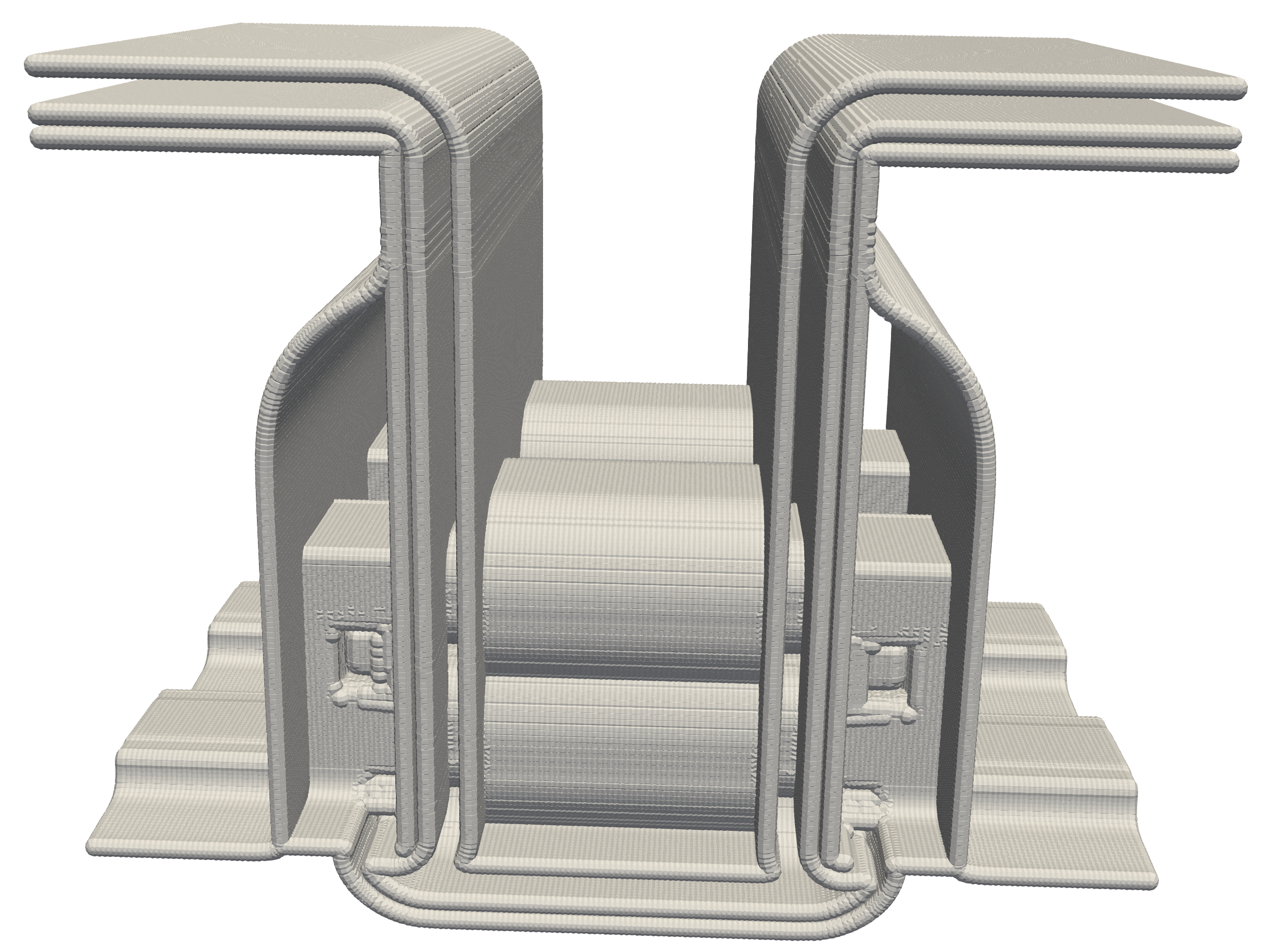
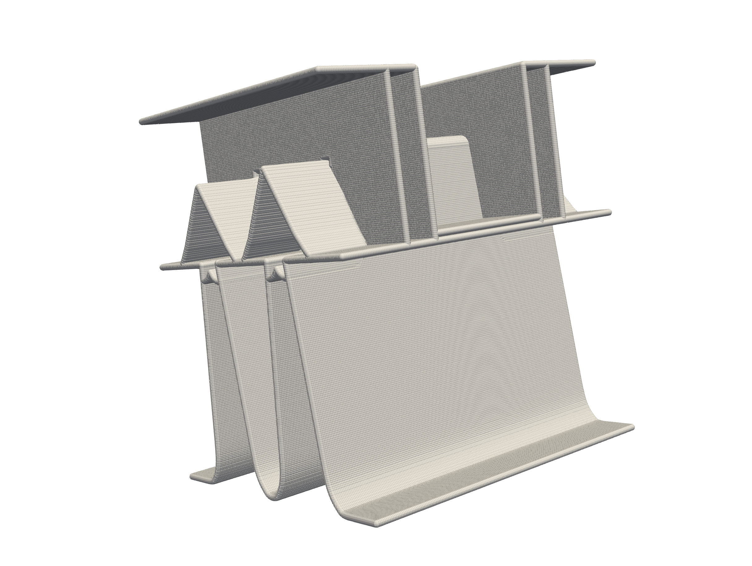
Figure 1.2 shows two examples of discretized topographies of modern semiconductor devices.
Figure 1.2: Examples of two discretized semiconductor device topographies.
Obviously, the quality of the discretization directly relates to the quality of the resulting topography. However, three additional aspects must be considered: First, not all parts of the topography of a semiconductor device benefit
equally from a high-quality discretization (e.g., flat parts). Second, the higher the discretization quality, the higher the impact on computational performance. Third, the choice of discretization is important as it has to be tailored
to the actual use case, i.e., different types of subsequent numerical processing steps require a specific discretization for optimal execution, as will be discussed in the following.
Discretization strategies of surfaces can be broadly categorized into parametric, implicit, and explicit representations [14]; this work focuses on the
latter two. Implicit representations define a set of points (i.e., a surface) that satisfies an equation of the form \(f(x,y,z) = c\), which is used to represent the topography of the semiconductor device. In the here considered
topography simulations utilizing the so-called level-set method, the implicit function is expressed as a level-set function. Level-set functions are usually discretized on a grid that stores the distance to the surface, because
it allows for an efficient and robust handling of surface deformations [8, 15].
Explicit representations directly describe points, or even entire regions, of the discretized domain. An example of an explicit surface representation is a surface mesh which discretizes a surface by covering it with interconnected
polygons (e.g., triangles) [16]. As indicated before, depending on the prerequisites of a given simulation, different surface representations have
benefits over others [17, 18].
The surfaces depicted in Figure 1.2 show that semiconductor device topographies are characterized by relatively vast areas with little to no geometric variation
(e.g., the flat areas of the topography) and comparably fewer parts with significant variation (e.g., the corners of the topography). As discussed previously, the parts of the device topography with significant geometric variation
benefit from a higher quality discretization, while the other parts do not, as it would introduce unnecessary considerable computational overhead. These observations motivate the use of a domain discretization that adaptively
increases the quality of the discretization depending on the geometric variation of the topography [19, 20, 21, 22, 23, 24]. A typical
adaptive data structure used in process TCAD is a hierarchical grid. Hierarchical grids consist of a base grid and a plethora of nested grids at various resolution levels to realize a locally higher resolution of the discretization. These
nested grids can be manually or automatically placed inside the simulation domain. As the topography changes during the simulation (e.g., simulating the gradual etching of a trench), the nested grids need to be continuously
adapted, requiring a metric which allows for measuring the topography variation.
A well-known metric, originating from the field of differential geometry, is the surface curvature. The surface curvature measures the variation of a surface in a small neighborhood around a point on the surface [25, 26, 27, 28, 29]. The surface curvature is thus in principle ideal for the automatic classification of parts of the surface. The concept of the surface curvature of a
differentiable surface can be discretized to encompass discrete surfaces, which allows this concept to be used in the here considered context. The surface curvature can be used to develop geometry-aware algorithms that
allow to focus computational efforts on parts of a discretized surface that benefit from a higher quality of the discretization (i.e., features).
On the one hand these geometry-aware algorithms can be used to increase the resolution of the simulation domain at parts with significant geometric variation, on the other hand this information about the surface can also be used
to decrease the resolution of parts of the simulation domain with little to no geometric variation. An important simulation step during a topography simulation is the so-called surface flux calculation. The surface flux describes how
much of a reactant (e.g., an etchant) interacts with the surface during a simulation step. One strategy to estimate the surface flux is Monte Carlo ray tracing [30]. Monte Carlo ray tracing can be efficiently performed on surface meshes which can be extracted from level-set functions. However, these contain an impractical
amount of triangles in flat regions of the topography, which increases the run-time of Monte Carlo ray tracing. Therefore, surface mesh simplification algorithms are used to reduce the number of triangles to improve performance.
Furthermore, the adaptation of the resolution of the simulation domain may not only be guided by geometric features of the topography, but may also be guided by other metrics. Many semiconductor devices like 3D NAND flash
memories or light-emitting diodes (LEDs) are fabricated by depositing thin material layers on top of each other [31, 32]. These stacked thin material layers are affected by subsequent processing steps like etching processes that create patterns on the device topography, or
separates individual devices that have been fabricated on the same wafer. During the simulation of etching process steps on thin material layers, numerical artifacts occur due to an inadequate resolution of the simulation domain,
which again can be mitigated by the use of hierarchical grids.
1.1 Research Goals
The primary research goal of this work is the formulation of a general algorithm that automatically detects parts of the wafer surface that benefit from a higher discretization of the simulation domain. This general algorithm is then
used to, on the one hand, guide a hierarchical grid placement algorithm to selectively increase the resolution of the simulation domain at critical points to improve simulation performance while minimizing computational overhead.
On the other hand, this algorithm is used to selectively coarsen surface meshes to maintain a higher resolution at critical parts of the device topography. The coarsened meshes are then used to accelerate surface flux calculations
required to accurately simulate the effects of specific processing steps on the wafer surface. Furthermore, different methods of calculating the curvatures (i.e., the metric used to analyze the wafer surface) on level-set functions are
investigated, and two complementary methods (i.e., performance focus, numerical accuracy focus) are obtained. Another important goal is formulating a specialized feature detection algorithm for thin material layers affected by an
etching simulation.
Research Setting
The research presented in this work was conducted within the scope of the Christian Doppler Laboratory for High Performance TCAD. The Christian Doppler Association funds cooperation between companies and research
institutions pursuing application-orientated basic research. In this case, cooperation was established between the Institute for Microelectronics at the TU Wien and Silvaco Inc., a company developing and providing electronic device
automation and TCAD software tools. The computational resources of the Vienna Scientific Cluster have been utilized during this work.
1.2 Thesis Outline
Chapter 2 gives a theoretical overview and reviews the discrete surface representations used in this thesis. Surface representations are
defined, and approaches to calculate geometric properties for each surface presentation are introduced. Furthermore, it is discussed how a surface that is given in one representation can be transformed into another
representation.
Chapter 3 introduces the mathematical concept of curvatures of a differentiable surface and their discretization for different
surface representations. Several methods for calculating the surface curvature of discrete surfaces are reviewed. The surface curvatures are the primary metric that is used throughout this thesis to detect features of the considered
geometries.
Chapter 4 reviews a typical topography simulation workflow as a frame of reference. It is discussed how the surface
representations introduced in Chapter 2 are used during a topography simulation. The representation and evolution of different
materials are introduced. Moreover, various strategies for surface flux calculations are presented. In the last part of this chapter, a brief overview of the used computer hardware and software tools in this thesis is given.
Chapter 5 introduces a new feature detection algorithm which is based on the surface curvatures. Different strategies for
calculating the surface curvature on level-set functions are discussed. The investigation focuses on the qualitative results of the feature detection on the one hand and on the run-time on the other.
In Chapter 6, it is shown how the hierarchical grid placement is directed by the algorithm presented
in Chapter 5. Furthermore, it is demonstrated how the performance of a practically relevant epitaxial growth simulation
is improved.
Chapter 7 introduces a new algorithm for detecting features that occur when performing Boolean operations
with thin material layers. Additionally, this algorithm is able to suggest a required minimal resolution to represent thin material layers after an etching simulation properly.
Chapter 8 introduces a new surface mesh simplification algorithm. This algorithm also uses the
feature detection algorithm presented in Chapter 5 to guide the simplification process. The performance of surface
meshes simplified with the algorithm is investigated in the context of flux calculation with Monte Carlo ray tracing.
Finally, Chapter 9 concludes with a summary of this thesis and presents ideas for future research.