

Computation of Torques
in Magnetic Tunnel Junctions
Chapter 2 Spin-Transfer Torque MRAM
The following chapter gives a brief overview of the development and working principles of MRAM, with particular focus on STT-MRAM. The contents are mostly based on the review papers [26], [27], and [28].
The history of random access memory began in the middle of the 20th century, when Williams Kilburn developed a system to store bits as electrically charged spots on the face of a cathode-ray tube [29]. In the 1950s, this early memory technology was replaced by magnetic core memories, where the data was stored in the rotation sense of an array of magnetic rings [30]. Magnetic core memories were largely employed for about two decades, until they were replaced by dynamic random access memory, based on newly developed semiconductor
technology. The new memory provided increased scalability, could be easily mass-manufactured and could be employed in the then-emerging integrated chips [31].
Interest in a magnetic approach to RAM grew again with the discovery of the giant magnetoresistance (GMR) effect in 1988 [32], [33]. The effect arises in a cell composed of two ferromagnetic layers with a nonmagnetic conductive metal between them. It describes the difference in the resistance when the magnetic moments of the two layers are parallel or anti-parallel to each other, with the parallel orientation having lower resistance. The higher the resistance ratio, the better the signal, enabling an easier detection of the written bits. The invention of magnetic tunnel junctions, where the effect is labeled tunnel magnetoresistance due to the underlying tunneling process, boosted research efforts in MRAM devices even further [34]–[39], thanks especially to the high TMR granted by using crystalline magnesium oxide as the tunneling layer [40]–[45]. First applications involving the GMR or TMR effect, however, relied on an external field to achieve switching of the magnetization direction, which prevents the scalability of the technology to small sizes and its application to high-density devices.
Such issue was overcome by the discovery of spin-transfer torque assisted switching. Magnetization reversal in STT-MRAM is achieved through purely electrical means, making it CMOS compatible and allowing a potentially faster switching capability, reliability, and scalability for future applications [14], [15], [46]–[50]. Thanks to these properties, research aimed at improving STT-MRAM to broaden its application range has been growing steadily and is still ongoing [2]–[8], [51].
2.1 Magnetoresistive RAM Working Principle
Magnetoresistive random access memory is a nonvolatile memory based on the magnetoresistance principle. The resistance dependence on the magnetization state is used as a way to retrieve the bit information, while the magnetic anisotropy energy is employed to retain the information. MRAM based devices have recently been released for niche applications, and researchers believe that MRAM could possibly replace SRAM and DRAM as technology progresses [1], [52].
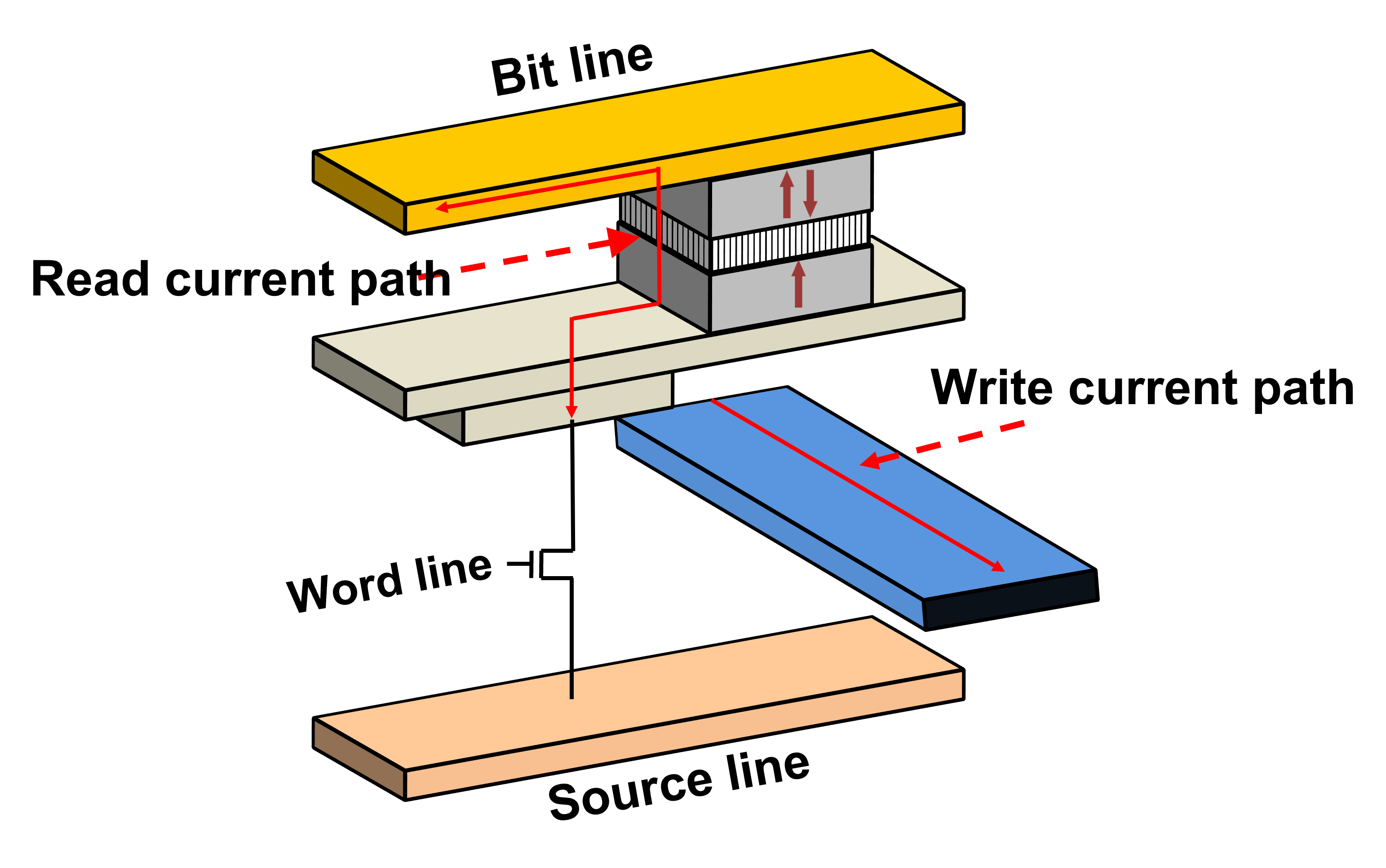
The first storage element used in MRAM was based on the GMR effect in a spin valve structure, which mainly consists of two ferromagnetic layers sandwiching a nonmagnetic conductive layer. The two FM layers are called the free layer and the reference layer, respectively. An antiferromagnetic (AFM) layer can be employed in proximity of or in contact with the RL in order to pin its magnetization direction, which should not be reversed during the operation of the memory device. For better functionality, a pinning layer (PL), antiferromagnetically coupled to the RL, can be employed to reduce the stray field, which may affect the FL stability.
More recent developments focus on the TMR effect in magnetic tunnel junctions, because of their superior reading signals. An MTJ cell consists of a thin layer of an insulating material, sandwiched by two ferromagnetic layers. Similar to a spin valve, the resistance states can be high (anti-parallel configuration) or low (parallel configuration), based on the relative orientation of the magnetizations in the RL and FL. MTJs have been the predominant storage element in MRAMs for the past decade, as they provide a difference between the resistance states significant enough to be suitable for RAM applications.
In an MRAM cell, the magnetization direction of the RL is fixed and only the one of the FL varies to store ‘0’ and ‘1’ bit states. Since the direction of the RL needs to be fixed during the switching process, it is made of materials
and shapes which ensure a higher energy barrier than the one of the FL. The FL magnetic anisotropy, albeit lower than the one of the RL, still needs to guarantee retention of the magnetization state for a given amount of years
(typically 10 at room temperature). Given an energy barrier
where
where
2.2 Magnetoresistance
Being able to read information is one of the most important criteria for new memory devices. The reading process of MRAM cells is based on the magnetoresistance effect, which relates the electrical resistance of certain materials or structures on their magnetization configuration. It is essential to achieve a high magnetoresistance ratio to make the MRAM more reliable, as a higher resistance difference between different magnetization configurations allows to more easily read the state of the memory.
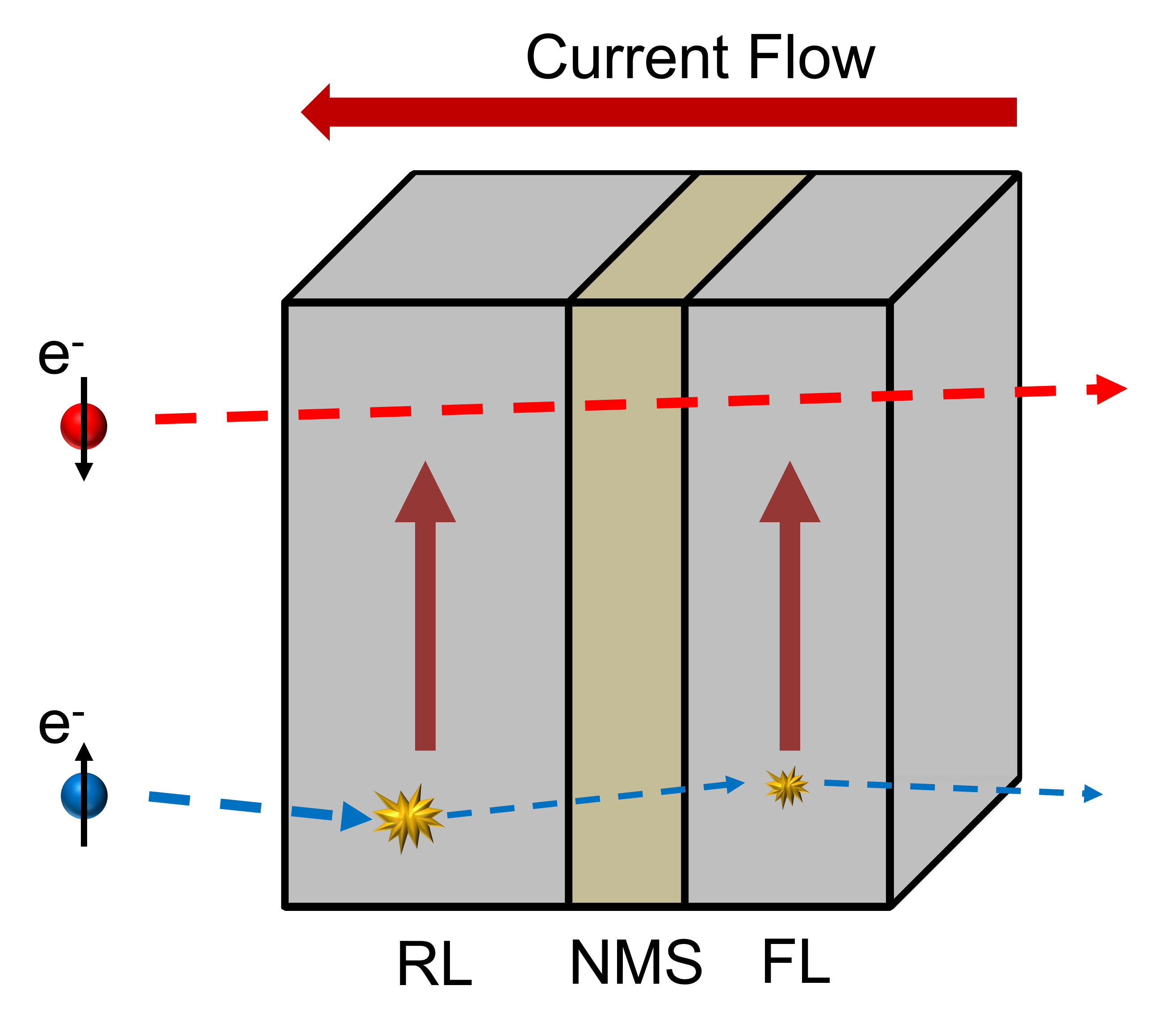
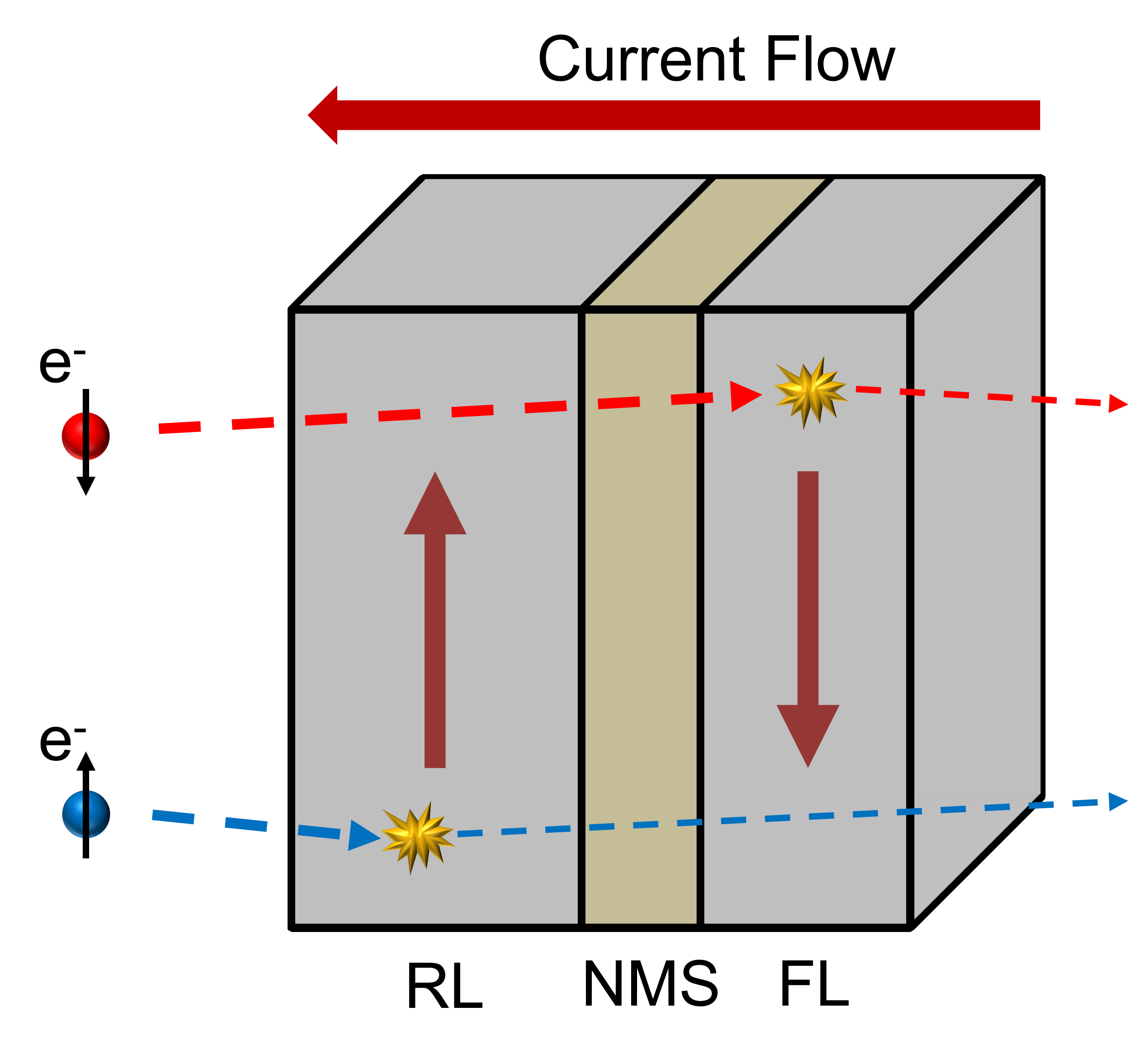
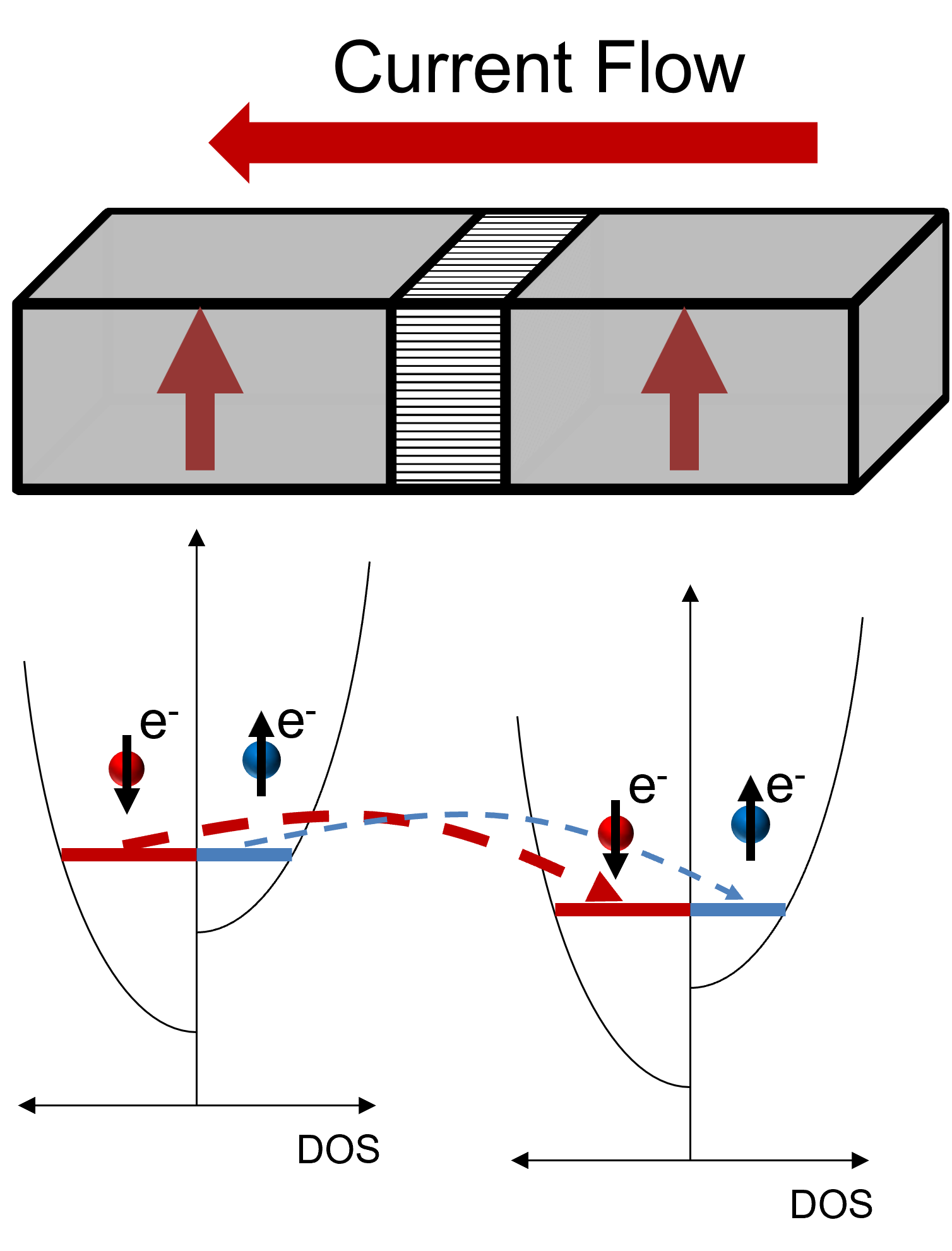
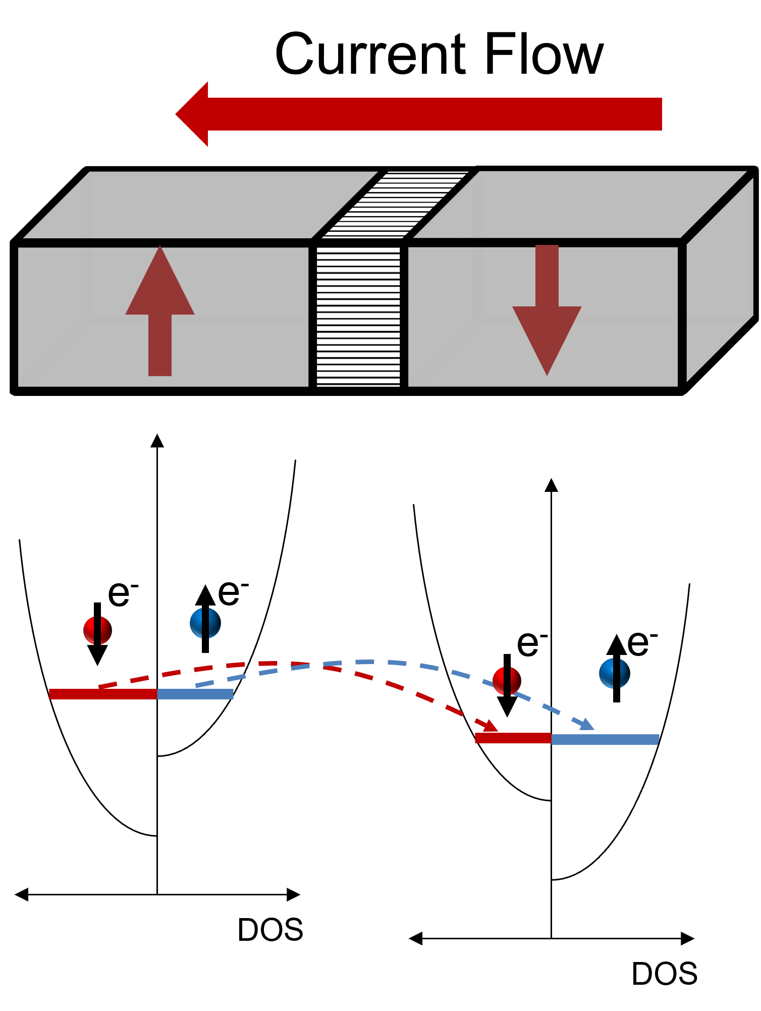
The discovery of the GMR effect and its application in the reading heads of hard disk drives was an important advancement, as high GMR values lead to improved reading signals compared to the ones given by the anisotropic magnetoresistance (AMR) effect [56]. The GMR effect is a consequence of spin dependent electron scattering. When the magnetic moments of two neighboring magnetic layers are aligned in an anti-parallel orientation, both the minority (spin parallel to the magnetization) and majority (spin anti-parallel to the magnetization) electrons are equally scattered when transiting through the structure. When the magnetization vectors are parallel, however, the majority electrons scatter less in comparison to the minority ones, so that a drop in the overall resistivity of the structure is observed. The process is schematized in Fig. 2.1. Spin-valve based devices relying on the GMR effect were suitable for hard disk applications. However, as the GMR ratio in these devices has never exceeded values of about 10–20% [57], [58], the difference between the high and low resistance states was not sufficient for MRAM applications.
The TMR effect, first reported at room temperature by Miyazaki et al. and Moodera et al. in 1995, was a major boost for MRAM applications [36], [37], with TMR values of about 20% using an amorphous Al
The main component of an MRAM cell based on the TMR effect is an MTJ, where two ferromagnetic layers sandwich a very thin insulating barrier, so that electrons can tunnel through it depending on the available free electron
states of the ferromagnetic layers. The resistance difference in an MTJ is caused by spin-dependent tunneling, and arises from the difference in the electronic density of states (DOS) at the Fermi level
where
2.3 Spin-Transfer Torque Writing
The second requirement of a memory device is that there must be a method to write data in the memory cells. The most straight-forward writing mechanism, and one of the first ones to be employed, is based on applying a magnetic field, which needs to be generated by an electric current flowing close to the MTJ. As the current density required to achieve the switching field increases when the cross-section of the line decreases [66], scaling of the memory cells towards smaller dimensions becomes troublesome. This limits the scalability of field-assisted MRAM devices (also referred to as toggle MRAM) to a size of about 90 nm [66], [67].
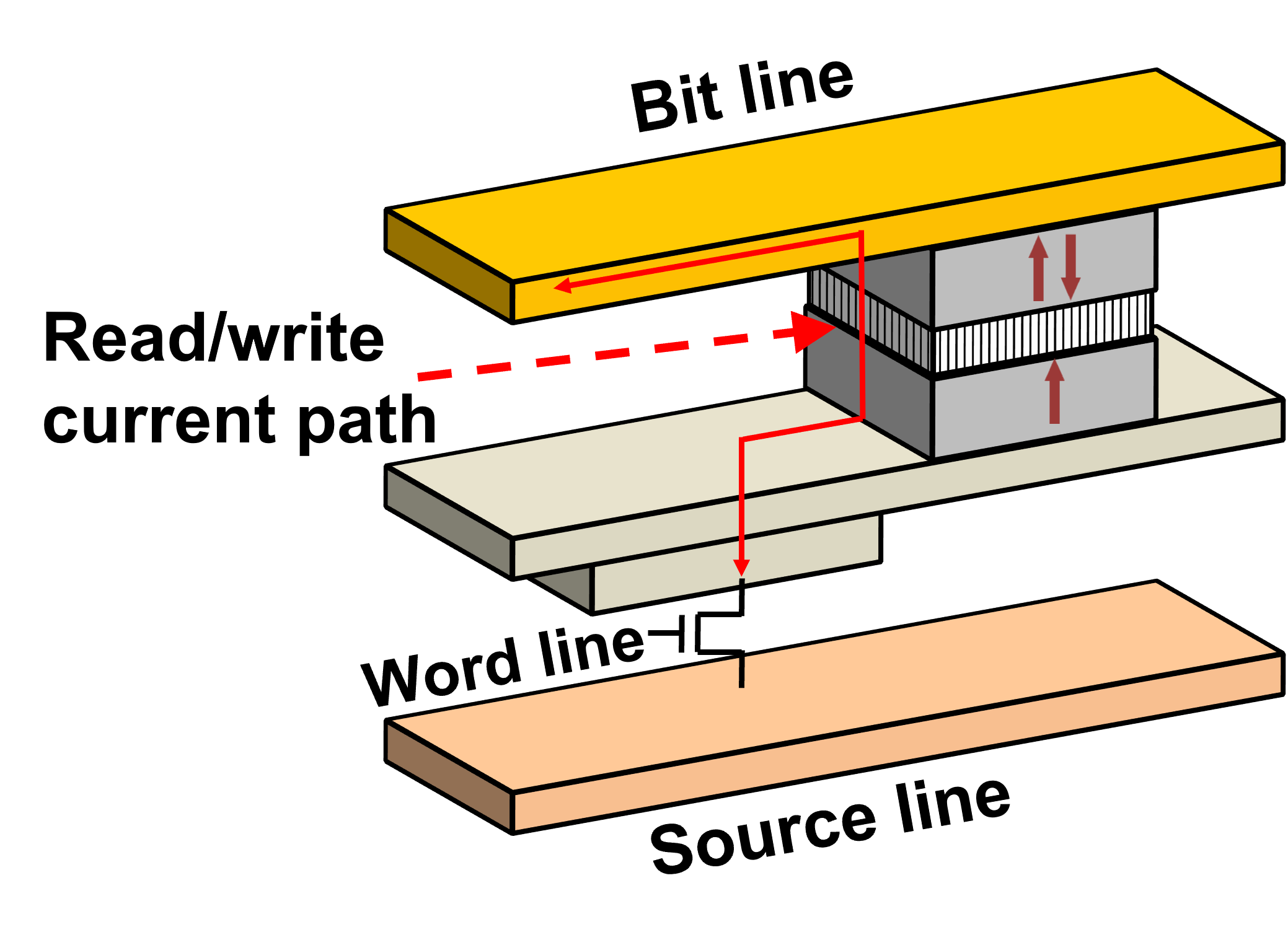
The predictions of STT, independently proposed by Berger and Slonczewski in 1996, paved the way for a purely electrical switching mechanism [14], [15]. The first demonstration of magnetization reversal induced by STT was presented by Katine et al. using a fully metallic spin valve device in 2000 [46]. The first STT-switching demonstration in MTJ-based devices was carried out by Huai et al. in 2004 on tunneling junctions employing an Al
where equation (2.2) was applied, and the critical current density by
Based on the storage mechanism, MRAM cells may be classified into two types: (i) in-plane MRAM, which has the magnetization of the ferromagnetic layers in the FL plane and (ii) perpendicular MRAM having the magnetization perpendicular to the FL plane [66].
In-plane MRAM was largely employed in the first generations of MRAM devices, as the magnetic fields generated in toggle MRAM lie in the plane of the films. In-plane MRAM cells are also easier to manufacture, as using an elliptic storage layer is sufficient to have a preferred orientation along the long axis, due to the shape anisotropy. The thermal stability of the FL can be enhanced by employing materials with uniaxial magnetocrystalline anisotropy. In order to keep the RL fixed, exchange bias is employed to pin the direction of the magnetization [72]. The RL is antiferromagnetically coupled to an additional magnetic PL, forming a so-called synthetic antiferromagnet (SAF). The magnetization of the PL in the SAF is pinned by direct contact with a layer of antiferromagnetic material. Such configuration allows to both boost significantly the stability of the RL, and to reduce the stray field acting on the FL [73].
In recent years, however, research interest has shifted to materials and structures possessing a perpendicular magnetic anisotropy (PMA) which enables the magnetization to have a stable configuration in the direction perpendicular to the plane of the magnetic film. Devices based on PMA present a better thermal stability and scalability, as well as a lower switching current, due to the fact that the path for electric switching and thermally-induced switching is the same in structures with magnetization perpendicular to the plane [12]. Several multilayered thin films have been studied in order to improve the properties of FLs with perpendicular magnetization [74]–[77]. It turned out that CoFeB which was predominantly employed for in-plane MRAM cells, possesses properties suitable for the fabrication of perpendicular MRAM cells as well. Results presented by Ikeda et al. in 2010 evidenced how PMA is present in MTJs based on thin films of CoFeB interfaced by MgO [53]. Perpendicular anisotropy in these systems is achieved due to interface effects between the CoFeB and MgO layer, and the annealing process is an important step to achieve both good PMA and high TMR [78]. As in the case of in-plane devices, the RL of perpendicular MTJs (pMTJs) is usually kept stable by antiferromagnetic coupling to an additional FM layer, forming a SAF. Due to the extremely high anisotropies achievable with materials exhibiting PMA, the pinning AFM layer is not necessary. Such SAF structures have been successfully and extensively developed and integrated into MgO-based pMTJ applications [79]–[81].
Further research has focused on improving the thermal stability as well as the switching properties, both by adding additional MgO layers to the structure [19], [82], and later employing elongated FLs to have a contribution from the shape anisotropy in the perpendicular direction [22]. This has led to practical pMTJ devices with the desired low switching current and high energy barrier needed for nonvolatile memory.