Computation of Torques
in Magnetic Tunnel Junctions
Chapter 5 Switching Simulations of Perpendicular STT-MRAM Under Fixed Voltage and Fixed Current Approaches
This chapter compares switching simulations of the FL of an STT-MRAM cell obtained by computing the torques under the fixed current and fixed voltage approaches previously introduced. The results hereby presented were
published by the author in references [110], [114], [115], and [116].
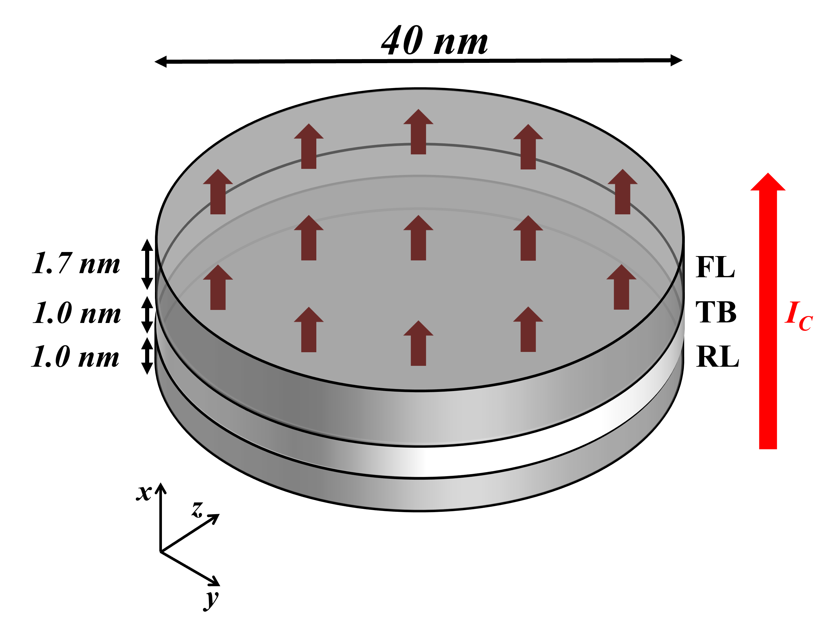
The simulations are carried out in the FL of a cylindrical pMTJ stack, with the system’s parameters set to match experimental structures [19], [53], [117]. The diameter of the stack is \(40\) nm, the equivalent thickness of the CoFeB FL and RL are \(1.7\) nm and \(1\) nm, respectively, and the thickness of the MgO TB is \(1\) nm. The cell size employed for the FD discretization is \(2~\times ~2~\times ~1.7\) nm\(^3\). A representation of the MTJ stack employed for these simulations is reported in Fig. 5.1. The perpendicular anisotropy provided by the interface between the CoFeB and MgO layers is reproduced using an uniaxial anisotropy contribution to the effective field. The interfecial anisotropy strength \(K_\text {int}=1.53\times 10^{-3}\) J/m\(^2\) is employed, giving an uniaxial anisotropy coefficient \(K=K_\text {int}/d_\text {FL}=0.9\) J/m\(^3\). The other contributions to the effective magnetic field \(\vb {H}_\text {eff}\) considered in this work are the external field, the exchange interaction, the demagnetizing field, the thermal field, and the stray field coming from the reference layer/magnetic stack. The simulations are carried out for the case were the TB polarization factor \(P\) is the same for the FL and RL. In order to account for the differences between the models, the value of the current employed for the fixed current approaches is set to \(I_\text {P}=V/R_\text {P}\) for simulations going from the AP to P configuration, and to \(I_\text {AP}=V/R_\text {AP}\) for switching from the P to AP configuration. \(R_\text {P(AP)}\) is the resistance of the MTJ in the P(AP) configuration, \(V\) is the voltage applied in the fixed voltage approach. The values of the parameters entering the LLG equation are reported in Table 5.1.
|
Parameter |
Value |
|
Gilbert damping factor, \(\alpha \) |
\(0.02\) |
|
Saturation magnetization, \(M_\text {S}\) |
\(1.2\times 10^{6}\) A/m |
|
Exchange constant, \(A\) |
\(10^{-11}\) J/m |
|
Perpendicular anisotropy coefficient, \(K\) |
\(0.9 \times 10^6\) J/m\(^3\) |
|
Thermal stability, \(\Delta \) |
67 |
|
Voltage, \(V\) |
2V |
|
Resistance Area, \(RA\) |
18 \(\Omega \) \(\mu \)m\(^2\) |
|
Parallel resistance, \(R_\text {P}\) |
1.4 k\(\Omega \) |
|
Antiparallel resistance, \(R_\text {AP}\) |
4.2 k\(\Omega \) |
|
Tunneling magnetoresistance ratio, \(TMR\) |
200 % |
|
Free layer surface area, \(S\) |
1257 nm\(^2\) |
5.1 Switching Realizations
With the setup described in the previous section, switching simulations are carried out employing the three proposed approaches to the current density computation. The time evolution of all three components of the magnetization
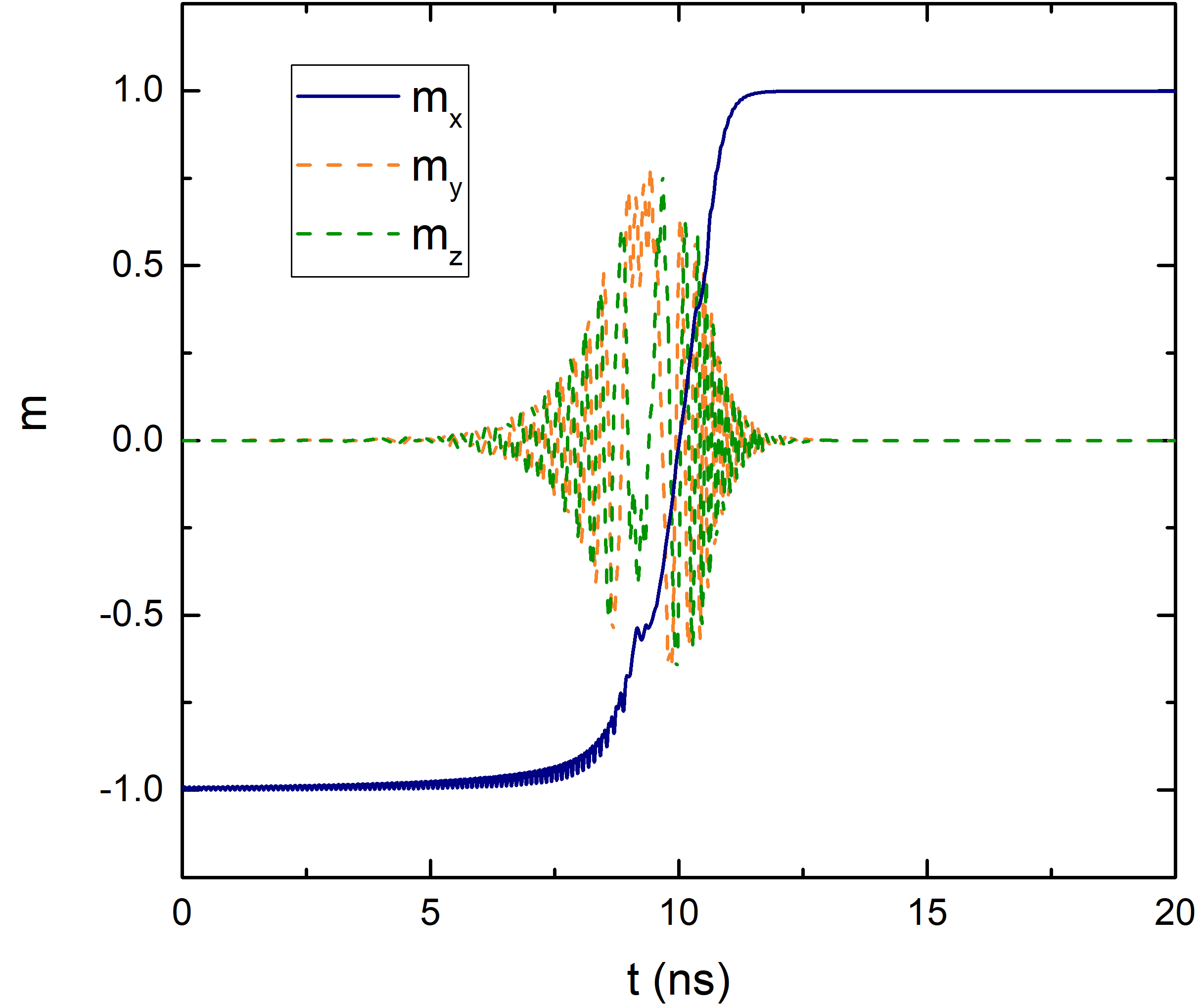
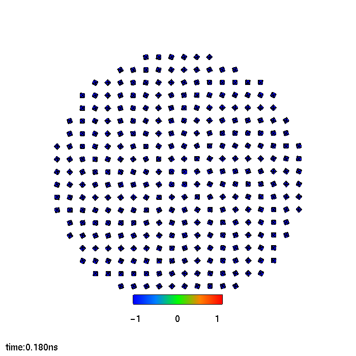
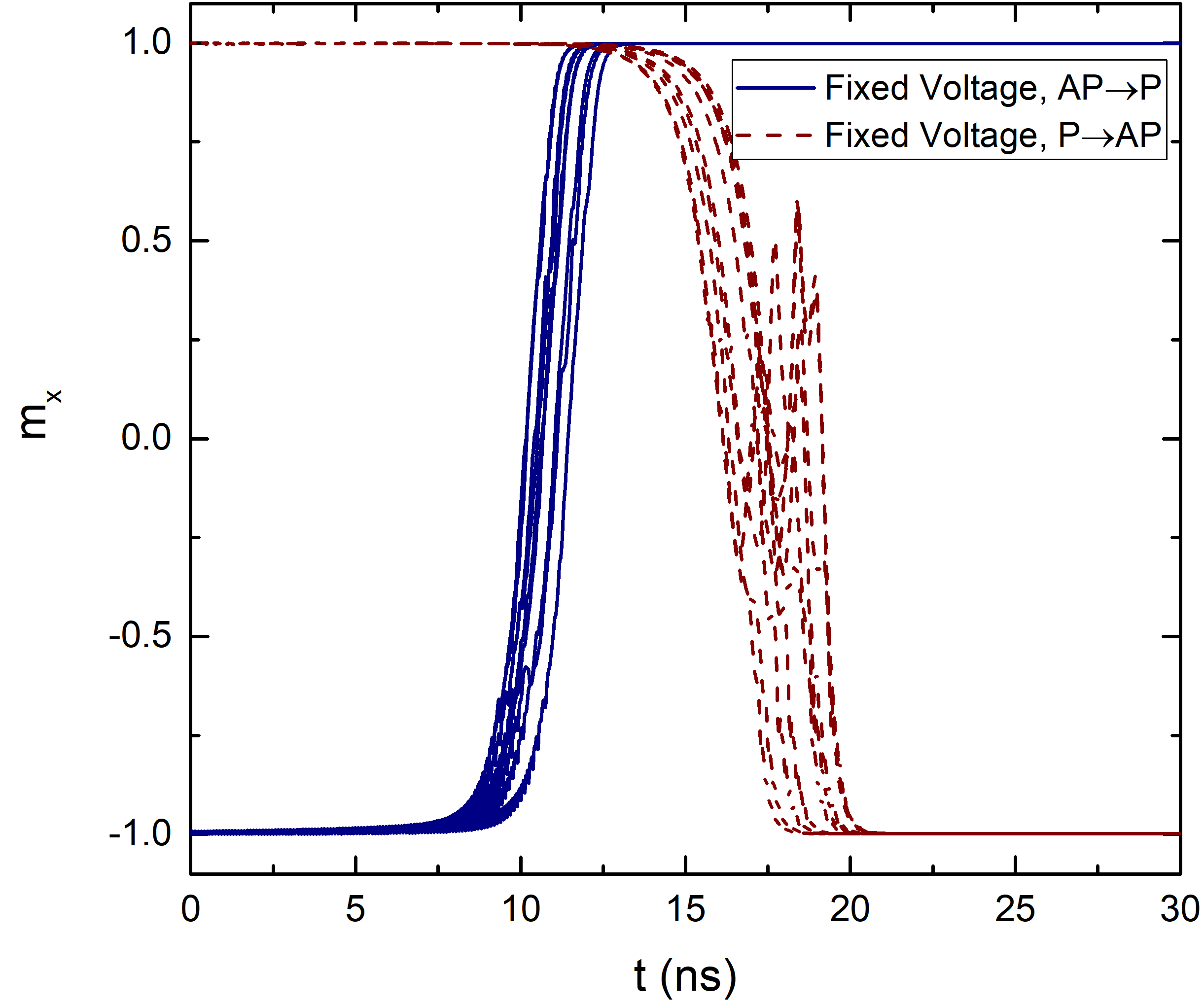
in a realization of the fixed voltage AP to P switching is reported in Fig. 5.2. After an incubation period of around 5 ns, during which the perpendicular component of the
magnetization stays close to the starting value of -1, the oscillations of the planar components of the magnetization increase and the switching process starts. The magnetization reversal takes about 5 ns, and then the
perpendicular component stabilizes at the end value of +1, parallel to the RL magnetization.
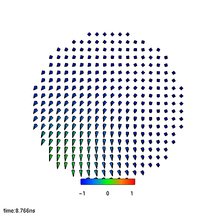
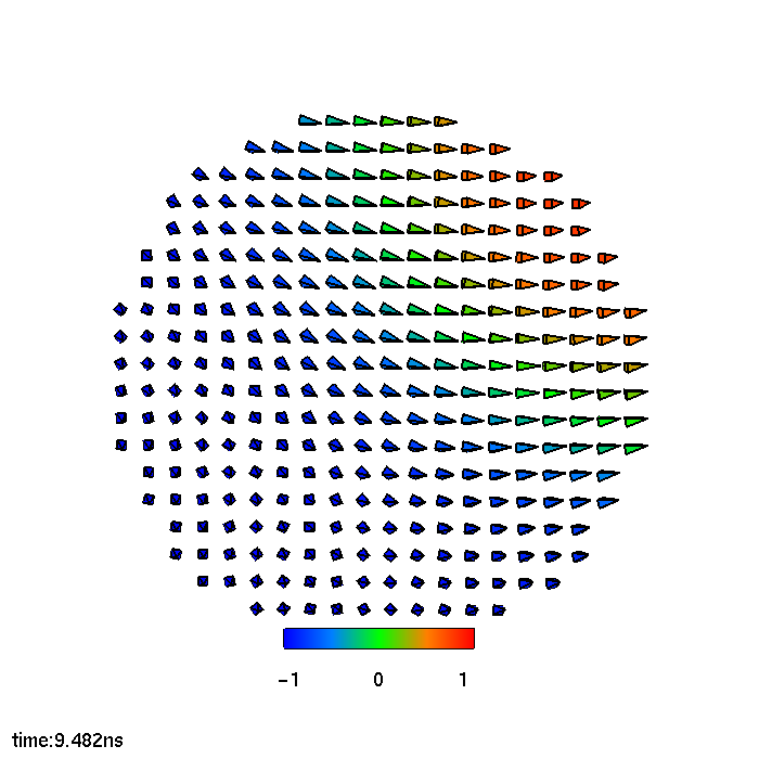
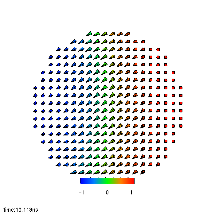
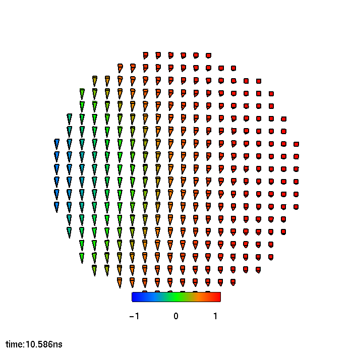
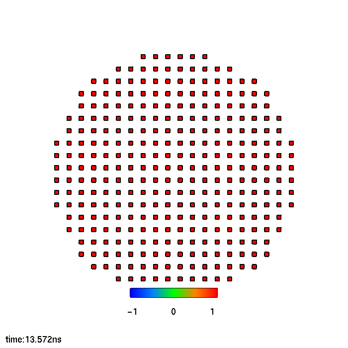
Fig. 5.3 showcases snapshots of the magnetization in the FL at different stages of the switching process. The magnetization reversal starts from the border of the FL, where the
action of the demagnetizing field, pushing the magnetization towards the plane, is the strongest. When the torque becomes strong enough to move the magnetization away from the -x orientation, the magnetic moments on the
external boundary start to oscillate, until a first seed of moments pointing to the +x orientation is generated. At this point, this region quickly expands to encompass the whole of the FL, completing the switching. From these
snapshots, it is clear how the magnetization is extremely non-uniform during the process, so that an investigation of the effects of the current redistribution is called for.
The simulation is carried out at the room temperature of 300 K. Due to the fluctuations of the magnetization under non-zero temperature, reproduced in the simulations by the thermal field contribution, every switching realization takes a slightly different path. A set of 10 realizations using the fixed voltage approach is showcased in Fig. 5.4. The different realizations present a similar behavior, but the start of the magnetization reversal happens at a slightly different time-step for each of them. It can be noted that the switching time required to go from P to AP is higher than that from AP to P. This is due to the uncompensated stray field of the RL, which tends to keep the magnetization of the two ferromagnetic layers aligned, helping the switching to the parallel configuration and opposing the switching to the antiparallel one. Due to this, during the P to AP process, even after the formation of the first region of reversed moments the magnetization can still undergo large oscillations before stabilizing along the antiparallel orientation. This can be observed in some realizations of the P to AP switching process, which present peaks in the trajectory of the perpendicular magnetization component.
5.2 Switching Time Comparison
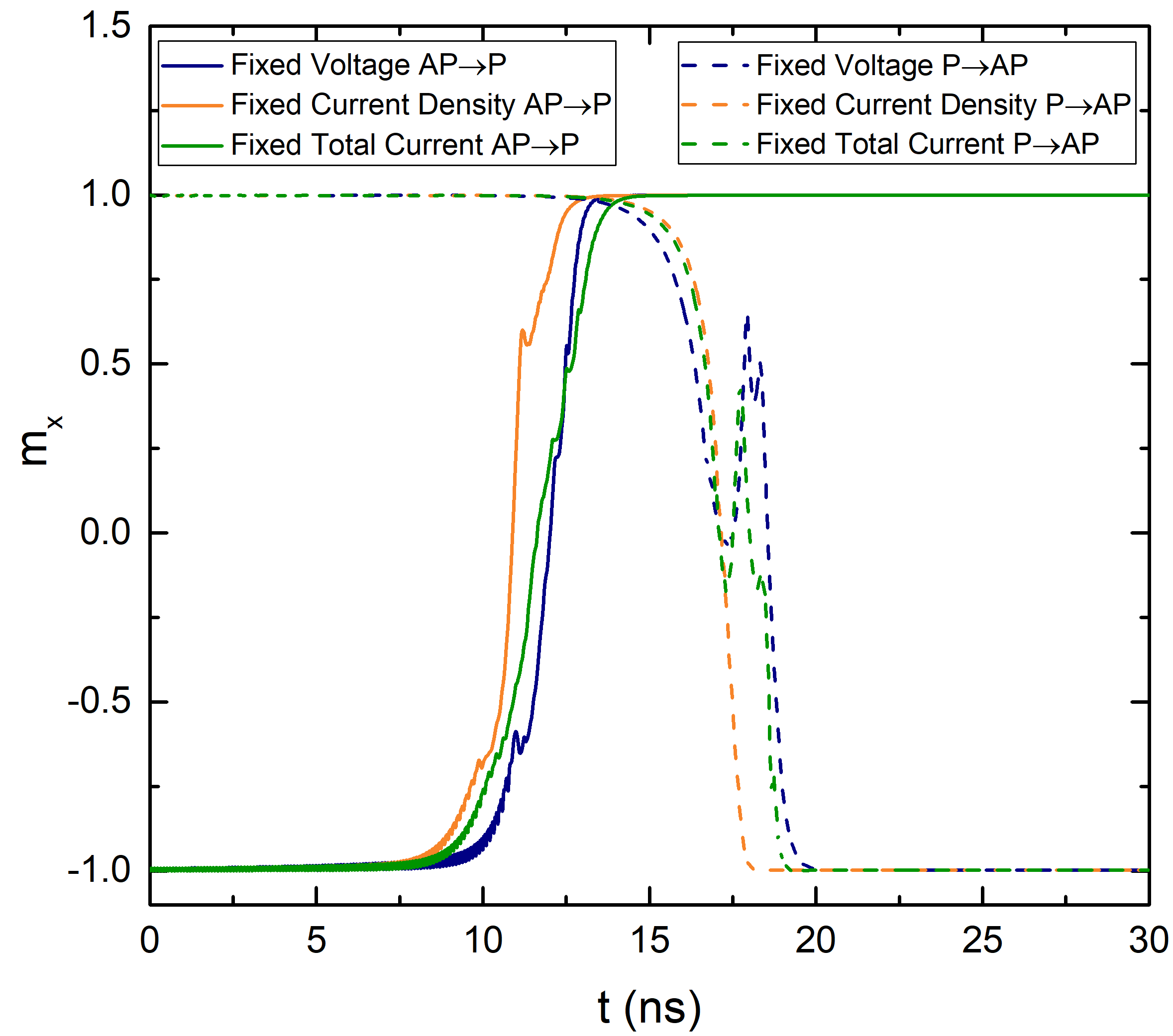
Examples of switching realizations for the three current approaches are shown in Fig. 5.5, for both AP to P and P to AP processes. A clear difference between the results can not be easily understood from looking at the magnetization trajectories of single realizations, due to the influence of the thermal field. The time required to complete the magnetization reversal, labeled switching time, can be a good indicator of the different performance of the models. As already discussed, the switching time difference between the AP to P and P to AP processes is due to the influence of the RL. By using a pinned layer antiferromagnetically coupled to the RL, the total stray field acting on the FL can be compensated, enabling a more symmetric switching process in the two magnetization configurations. The presence of the pinning layer is introduced in the simulations by modulating the total saturation magnetization of the antiferromagnetically coupled layers. The value of the combined saturation magnetization of the two layers is labeled \(M_\text {S,pin}\).
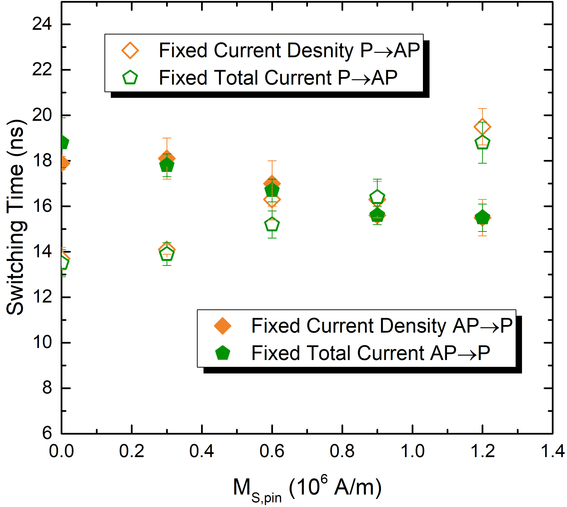
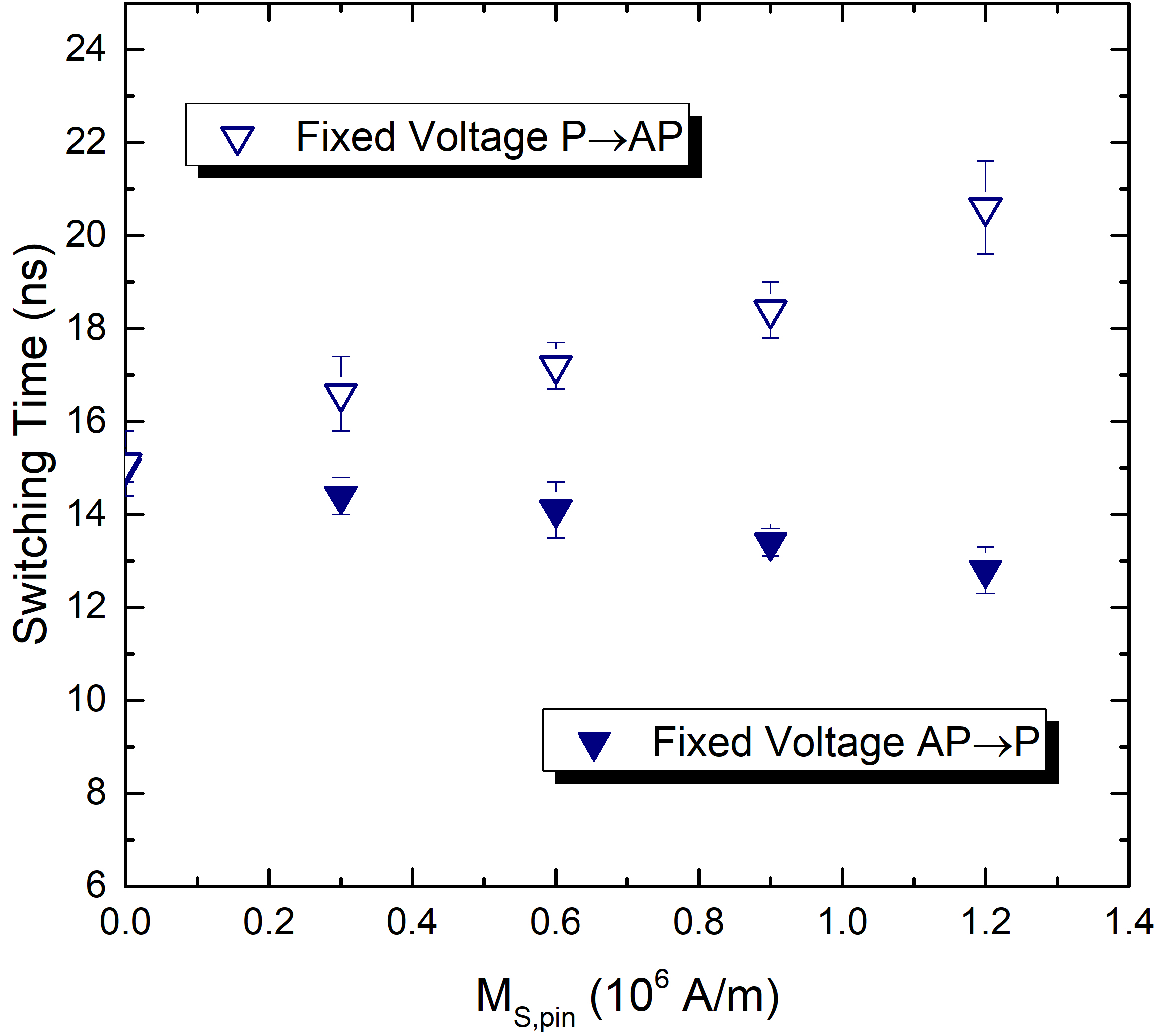
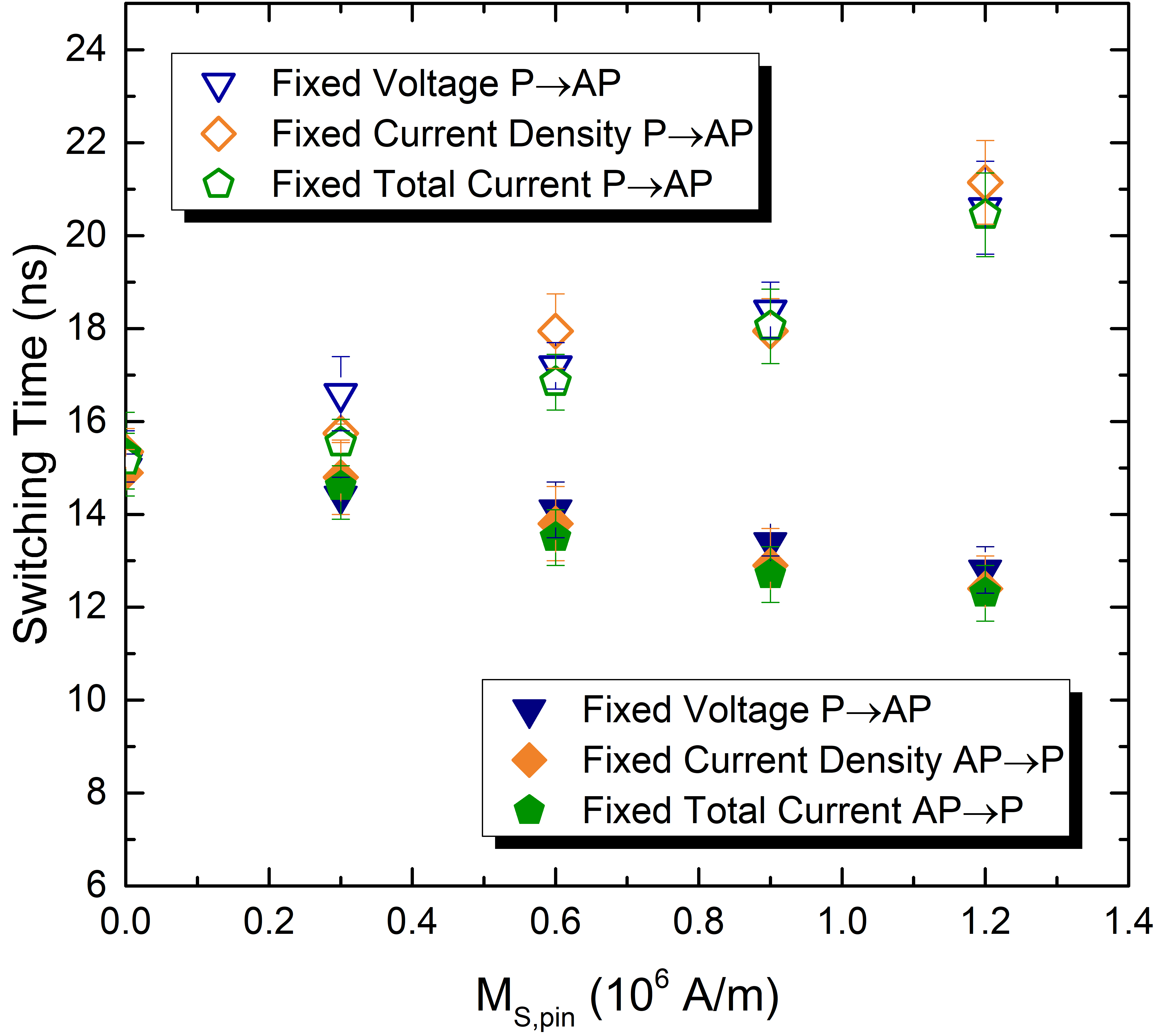
Fig. 5.6(a) reports the switching times as a function of uncompensated stray field. The switching time is taken at the end of the process, when the difference between the value of \(|m_\text {x}|\) and the maximum value of 1 is less than 5%. The results are averaged over 20 realizations, in order to take into account the effects of the thermal field. The error is taken as half the difference between the highest and lowest obtained values. As expected, compensating the stray field results in a higher switching time for the AP to P configuration and a lower one for P to AP. As shown in the figure, the average switching times assuming a fixed total current or a fixed current density are remarkably similar for both P to AP and AP to P switching. However, the switching for the fixed constant voltage looks quite different. The switching times are \(\sim 15\)% higher for AP to P and \(\sim 10\)% lower for P to AP for the fixed current approaches, as compared to the model with fixed voltage. This discrepancy is attributed to the fact that, when the voltage is fixed, the total current is allowed to vary according to the MTJ resistance, while the other two approaches have the same total current flowing through the structure during the whole reversal process. In order to compensate the effect of varying resistance, the total current value under the assumption of a fixed current must be increased by \(\sim 9\)% for AP to P and decreased by \(\sim 4\)% for P to AP switching. The resulting switching times are shown in Fig. 5.7: with this tuned choice of currents, all the models produce compatible results within the thermal spread.
The proposed current adjustment, albeit providing a feasible way of producing results compatible with a fixed voltage approach even in the more commonly implemented fixed current assumption, could depend on various system parameters, especially the TMR ratio and the dimensions of the stack. Further analysis and simulations are required in order to gather a better understanding of these dependencies. The analysis is performed in the next section.
5.3 Study of the Current Correction Dependencies
5.3.1 Dependence on the TMR at Room Temperature
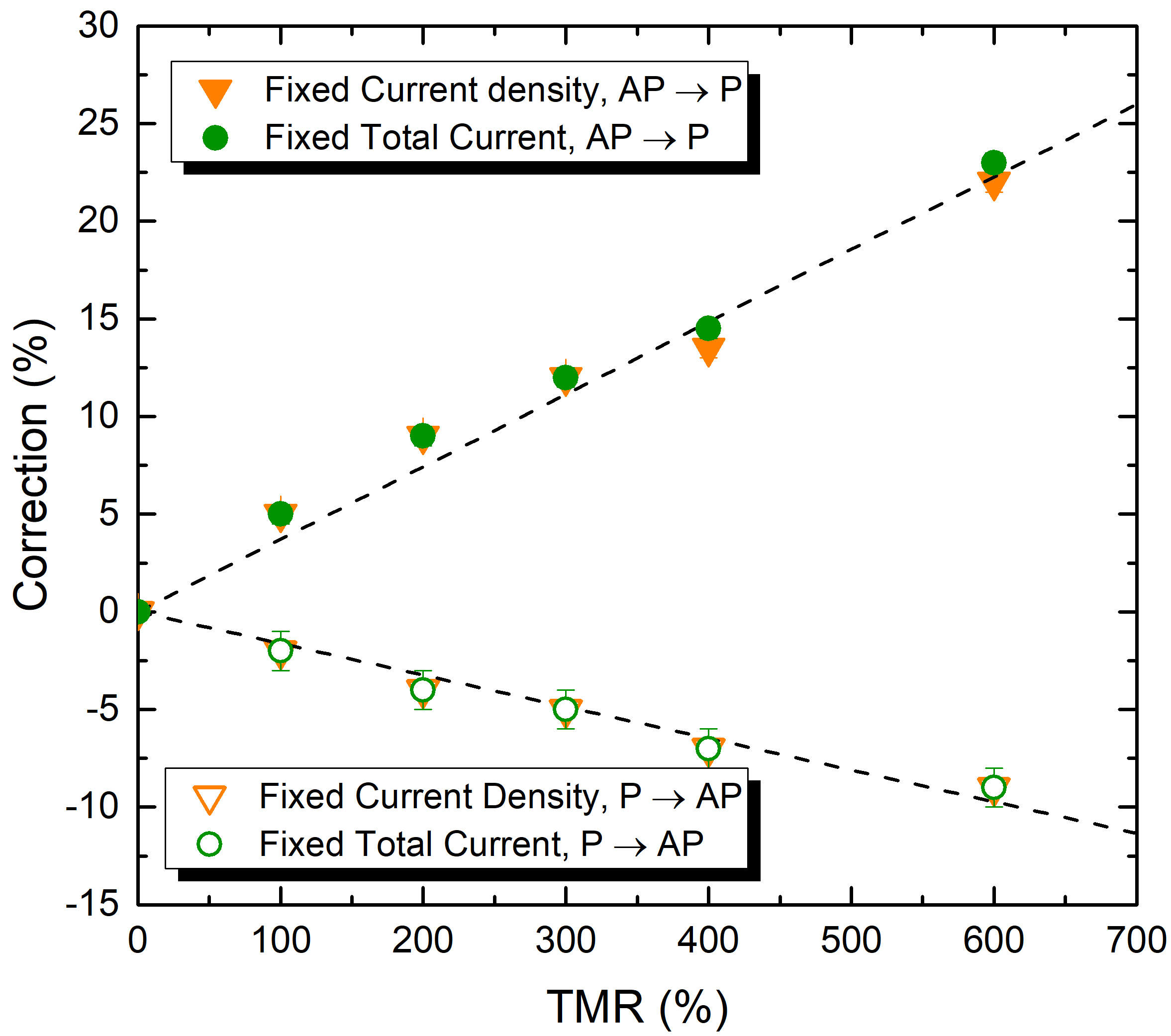
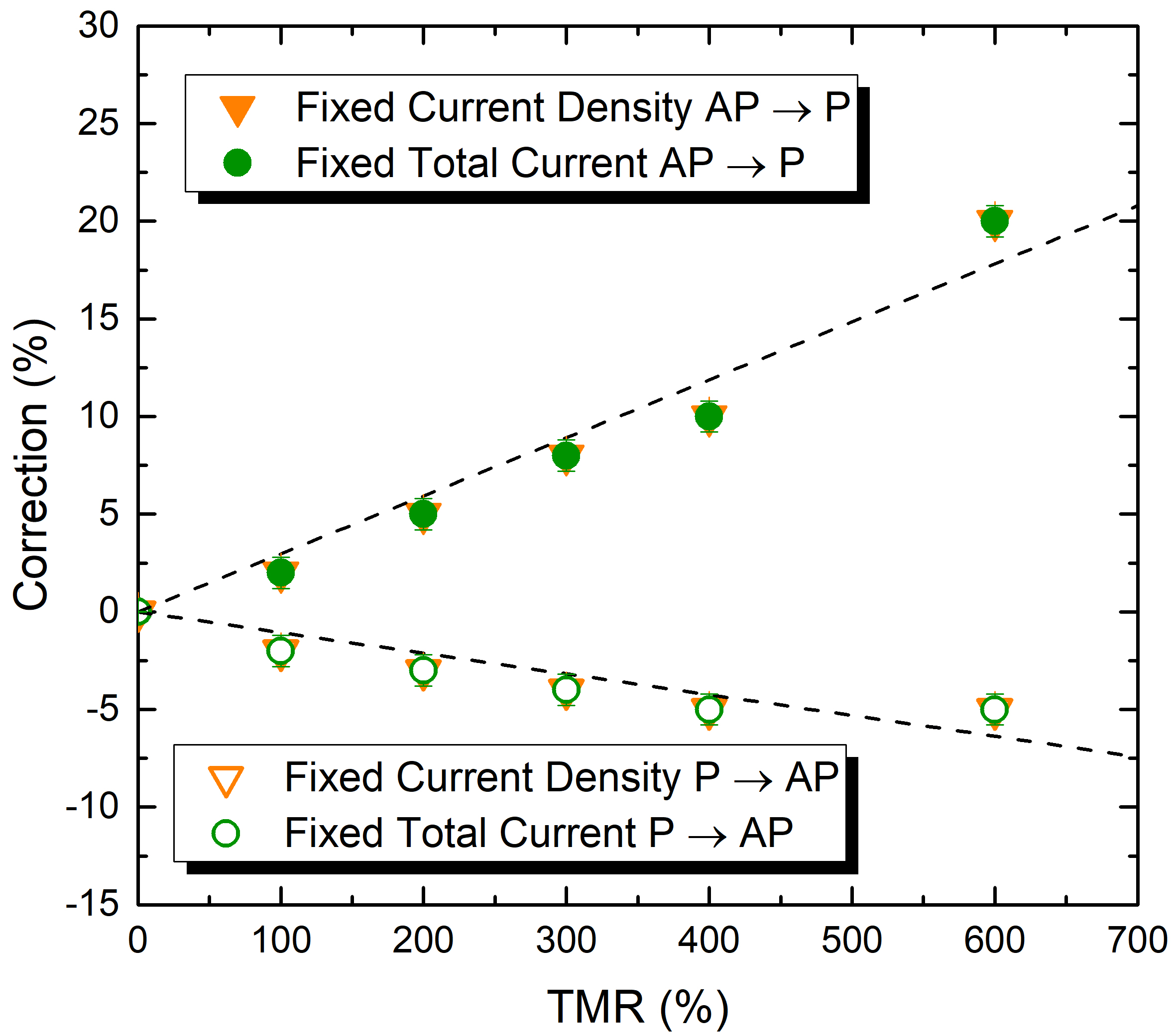
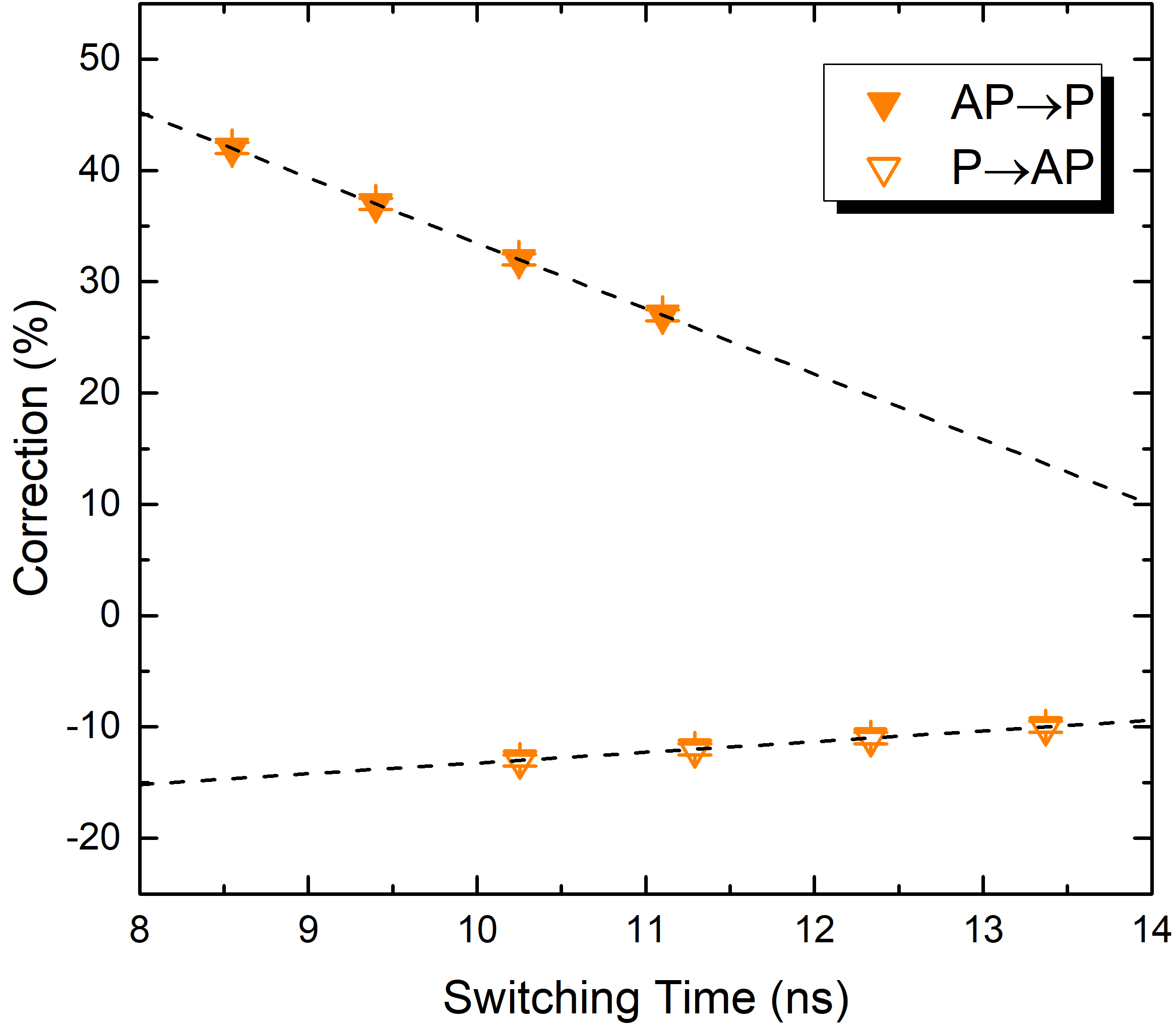
The TMR is arguably the most important characteristic of an MRAM device, as its value determines both the read performance and the torque magnitude through the Julliere formula (3.51). The dependence of the current correction on this parameter is thus investigated. The TMR is varied, while the others parameters are kept at the values shown in Table 5.1. The correction to the current value necessary to obtain a switching time comparable to the one at fixed voltage is evaluated for both fixed current approaches. The dependence of the correction on the TMR is shown in Fig. 5.8. The results imply that the constant current density assumption can be employed in the realistic case of switching at a constant voltage at room temperature, provided that the current is appropriately corrected for the P to AP and the AP to P scenario, and that the correction must be adapted to the TMR value. The obtained dependence can be well reproduced by a linear fit, as showcased by the dashed lines.
5.3.2 Dependence on the TMR at Zero Temperature
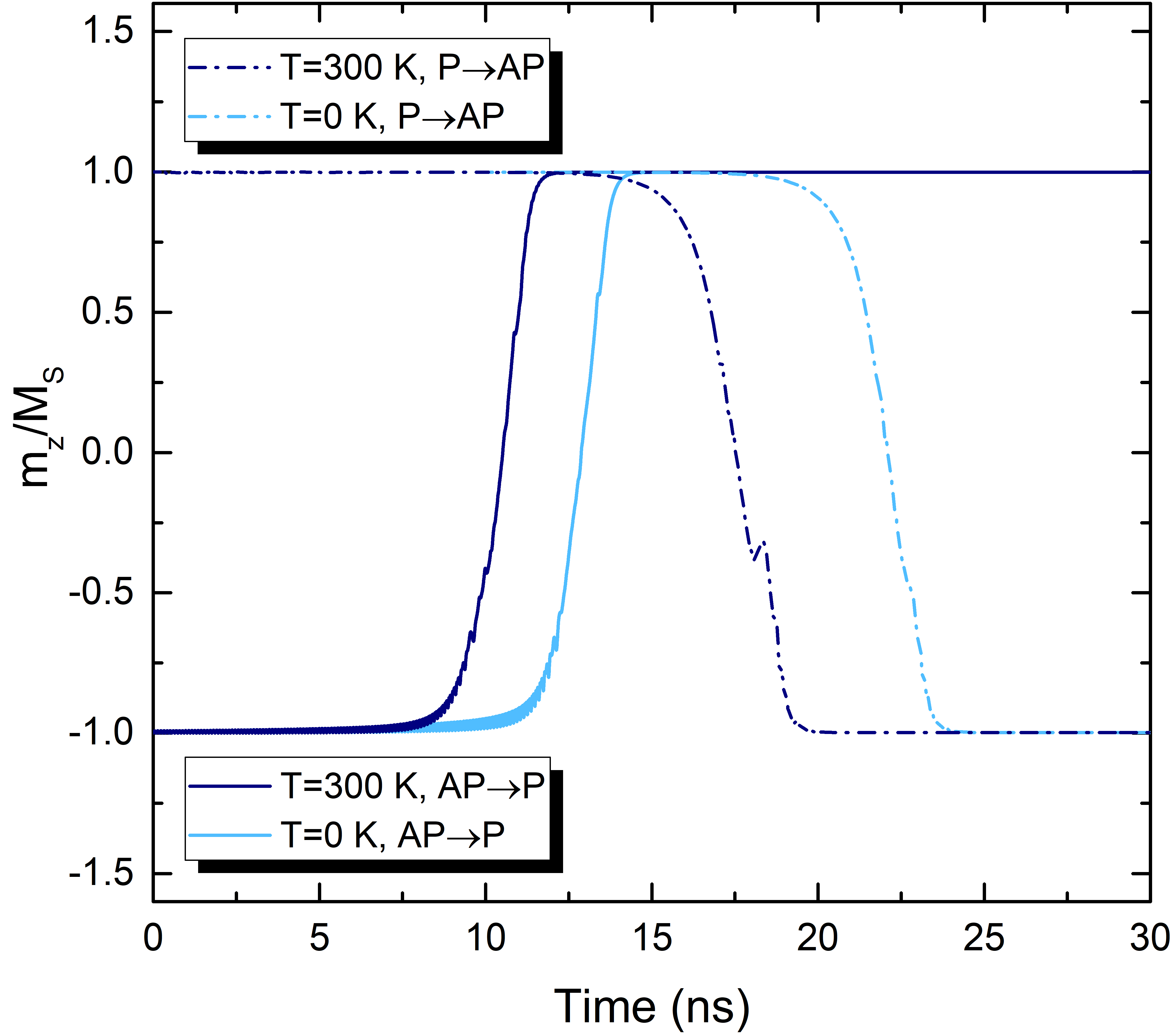
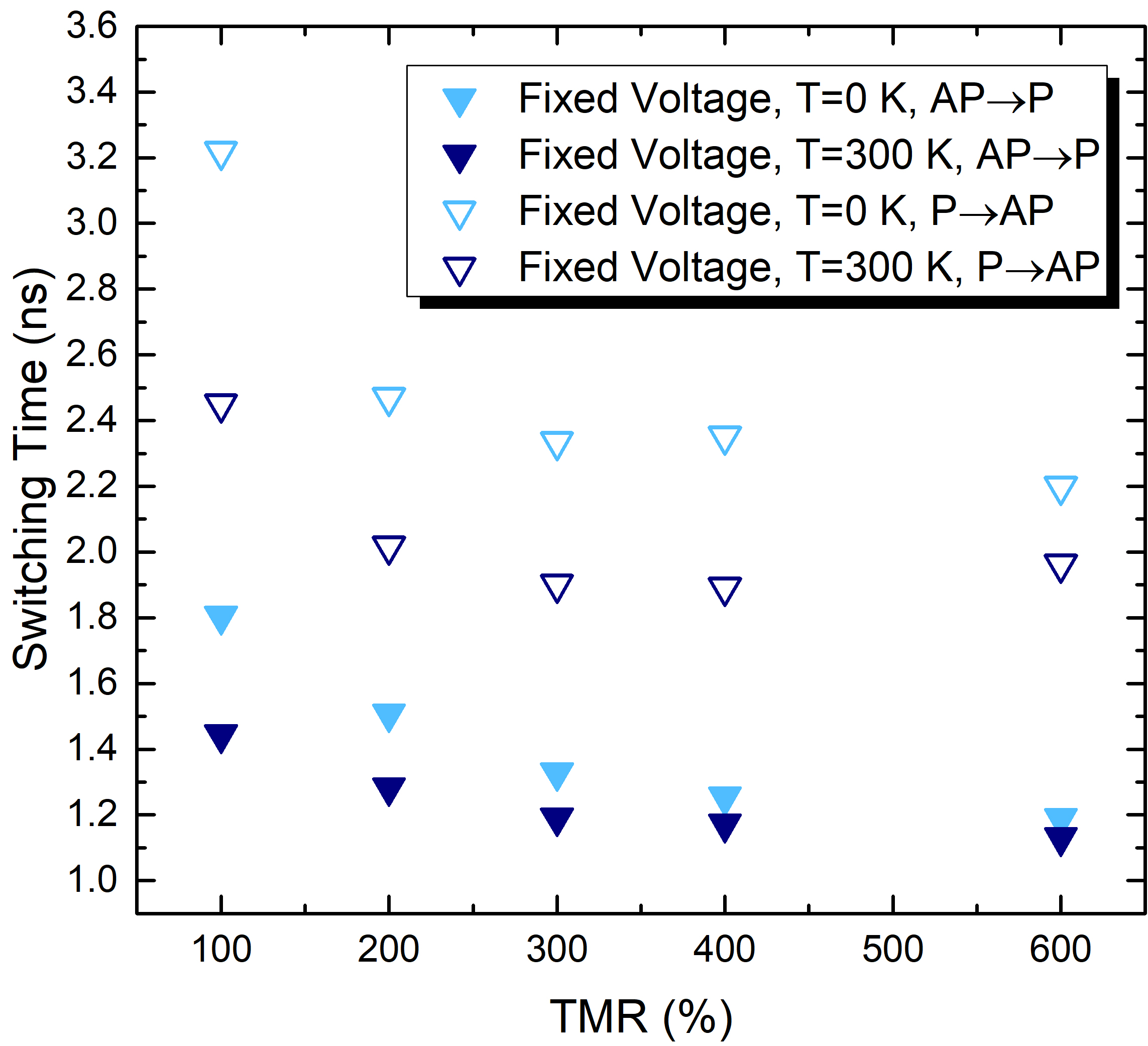
In order to further elaborate on the origin and magnitude of the current correction, the TMR dependence is computed again for the case of zero temperature, where the thermal field is not active and switching is deterministic. Like in the case of room temperature, the results for the switching time under the assumption of a fixed voltage differ from those with the fixed current. However, with the appropriate current correction, all three models provide similar results. The dependence of the correction on the TMR at zero temperature is reported in Fig. 5.9. The dependence still follows a linear trend, with the dashed lines reporting a linear fitting of the results. The current correction required is smaller than the one obtained at room temperature for all tested values of the TMR. It can be also noted that the switching process is faster at room temperature for both AP to P and P to AP processes, as depicted in Fig. 5.10. This happens because the stochastic thermal field helps to give the initial push to move the magnetization away from the parallel or antiparallel configuration, giving way for the torque to act on it and shortening the incubation period. Next, the switching time difference between room and zero temperature is investigated, at various values of the TMR. Results for both AP to P and P to AP switching are reported in Fig. 5.11. It can be observed that the switching time is always longer at zero temperature than at room temperature, as expected. Notably, the switching time shows also a clear dependence on the TMR, decreasing with higher TMR values. This dependence of the switching time on the TMR can be explained with the help of (3.50) and (3.51). The torque intensity increases with the polarizing factor due to the relation expressed in (3.50), while the polarizing factor increases with the TMR as described by (3.51). Thus, higher TMR values create a stronger torque, making the switching happen faster.
5.3.3 Macrospin Approximation
To have a deeper understanding of the possible reasons for the dependence of the current correction on the TMR and temperature, switching simulations are performed in the macrospin approximation, where the magnetization of
the whole FL is represented by a single vector. In the FD implementation, this is achieved by representing the FL as a single cell with dimensions \(40 \times 40 \times 1.7\) nm\(^3\). The simulations are carried out
at zero temperature. In the macrospin approximation, the nucleation process portrayed in Fig. 5.3 is not possible. Moreover, at zero temperature, the thermal field is not
acting, so that there is no contribution which can remove the magnetization from its initial parallel or antiparallel orientation. For this reason, the starting magnetization direction is slightly tilted, so that the STT torque can act
and achieve magnetization reversal.
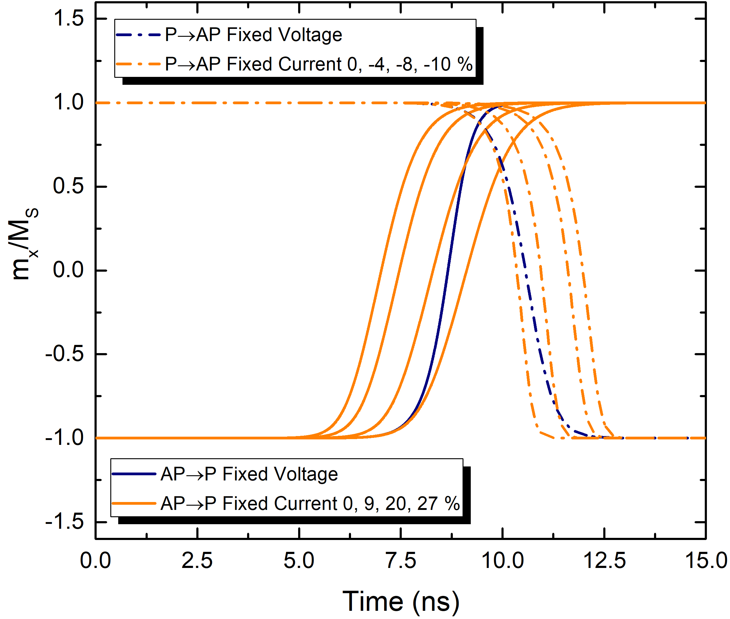
Fig. 5.12 presents results obtained from the fixed voltage and fixed current density approaches, for several values of the current correction and for both AP to P and P to AP
realizations. As only one magnetization vector is present, there is no possibility for current density redistribution in the fixed total current approach, and expressions (4.25) and (4.26) produce exactly the same torque. The macrospin simulations
demonstrate clearly that the switching process with a fixed voltage is steeper for AP to P switching than that with a fixed current. In order to compensate for the more gradual slope at fixed current and obtain similar switching
time, the switching process must start earlier, which is achieved by increasing the current value. For the switching from P to AP, with the fixed current model providing a steeper magnetization trajectory, the switching is slower in
the fixed voltage approach. Therefore, the current needs to be lowered to make the switching start later and compensate for the difference in slope, achieving similar switching time.
The difference in the switching trajectory between the two approaches can be explained by looking at equations (2.4), (3.50) and (3.51), describing the conductance, the torque and the relation between polarization and TMR
in an MTJ. In the model with fixed voltage the dependence of the current on the magnetization configuration, coming from (2.4), completely
compensates the angular dependence in the denominator of (3.50), so that the torque magnitude only depends on the sine of the angle between
magnetization vectors, coming from the vector product term [16], [99], [118]. Under the fixed current assumption, the denominator is not compensated, and it is minimal at the beginning of AP to P switching. At this point, the torque is the same as
under the fixed voltage assumption, due to the choice of having the same current at the beginning of switching in the two approaches. The denominator then grows larger as the configuration proceeds towards P, reducing the
torque. This trend must be compensated by a current correction to increase the initial value of the torque. The scenario is opposite for the case of P to AP switching, with the torque becoming larger as the magnetization proceeds
towards the antiparallel orientation, in agreement with the switching results of Fig. 5.12. The denominator is maximal at the beginning and becomes weaker during magnetization
reversal, and the trend can be compensated by employing a weaker current.
By gradually increasing the initial tilting angle, the switching process can be made faster without changing the system parameters. The dependence of the current correction on the switching time can thus be evaluated, as reported in Fig. 5.13. The data show that a faster switching requires a higher correction to the current value. As the average switching time is shorter at room temperature, it explains a slightly larger current correction required to match the results for switching times from all three models at T=300 K as compared to the simulations at T=0 K. It also explains the dependence of the correction on the TMR, as higher TMR values give a stronger torque and decrease the switching time for both AP to P and P to AP switching, so that the current correction required becomes higher.
5.3.4 Dependence on the Surface and Resistance Area
In order to corroborate these findings, switching simulations with different diameters of the stack, providing different surface areas, are performed at room temperature. As the resistance of a structure is inversely proportional to the
surface area \(S\), the total current, given by \(I_\text {C}=V/R\), is directly proportional to it. The current density is approximately given by \(J_\text {C}=I_\text {C}/S\), so its value does not depend on the lateral size of
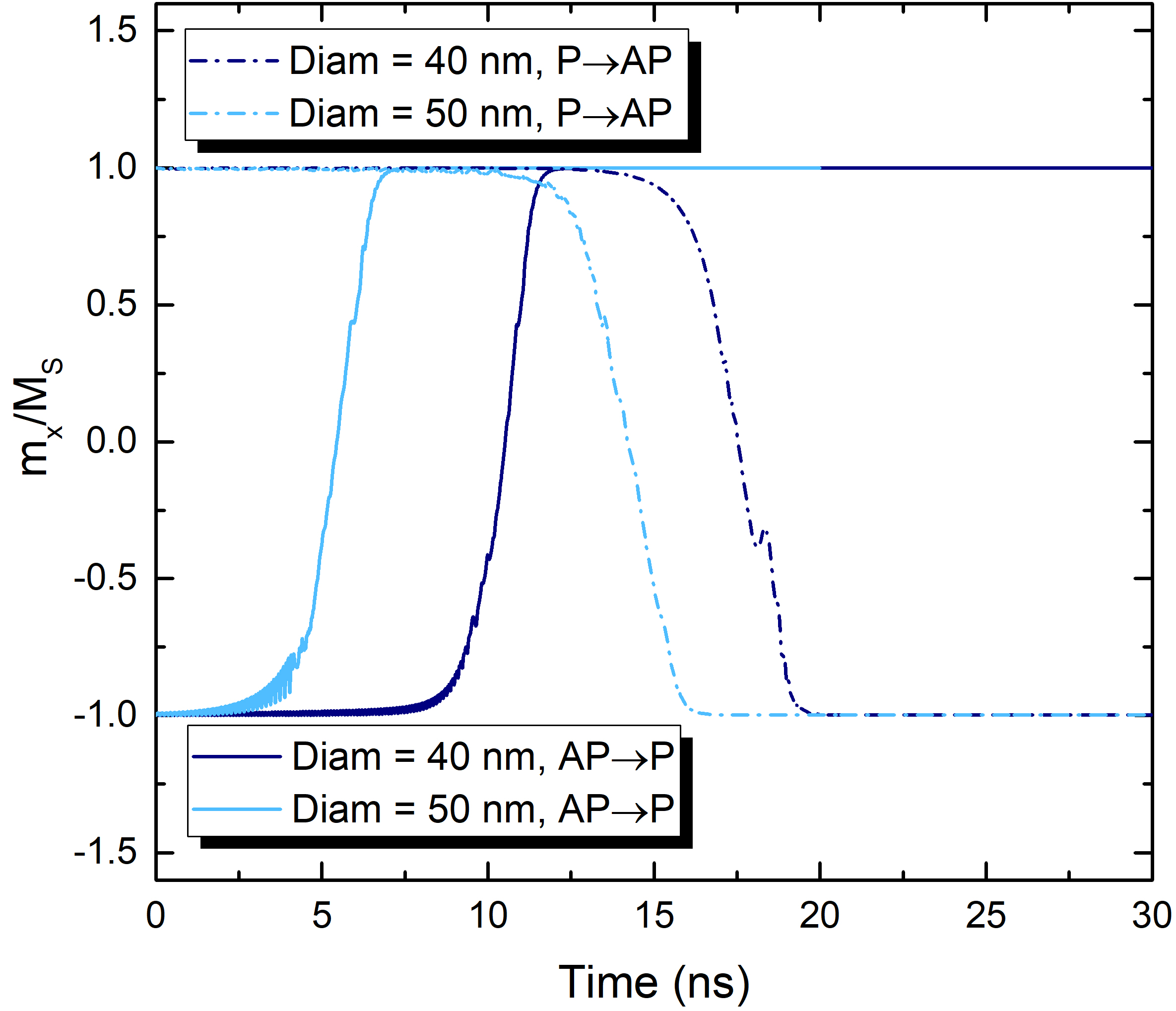
the MTJ. By keeping the same voltage employed for the previous simulations, the same current density is also maintained. Fig. 5.14 reports a comparison between switching
simulations performed at diameter values of 40 nm and 50 nm, providing a surface area value of 1257 nm\(^3\) and 1963 nm\(^3\), respectively. The results show how the magnetization reversal happens
faster in the wider stack, for both AP to P and P to AP realizations. when the lateral size of the junction is bigger, the resistance is lower, and the total current flowing through the structure is higher. Moreover, the nucleation of
domains with tilted magnetizations is easier for bigger diameters, as it is more difficult for the exchange interaction to keep the magnetization vectors in the whole layer aligned. This reduces the incubation time and creates an
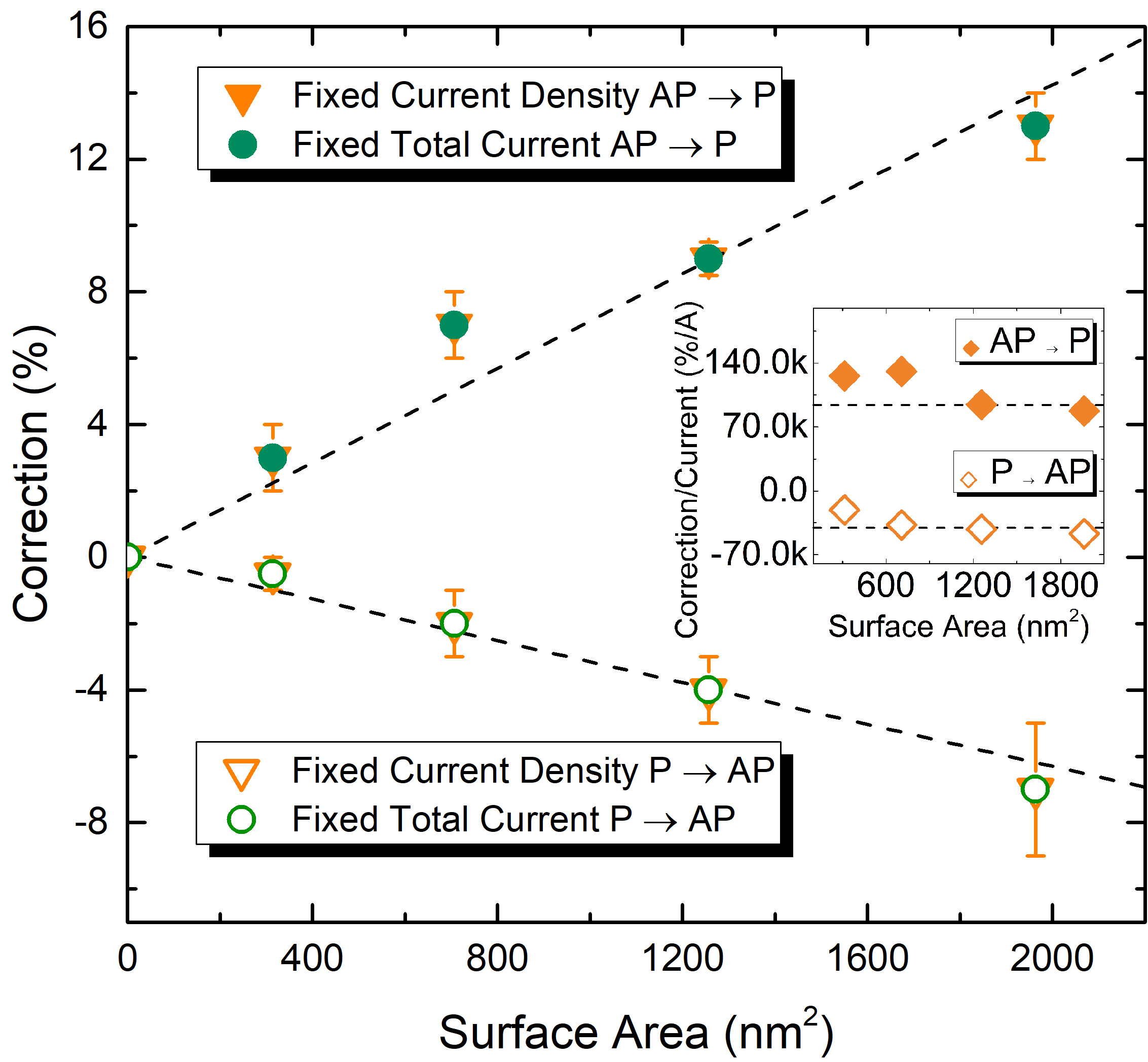
overall faster switching process. The dependence of the correction on the size of the structure is reported in Fig. 5.15, showing how the required correction is higher for larger surface
areas. The inset shows that the ratio of the correction on the current value does not depend on the area, underlining how the correction increases with the total current.
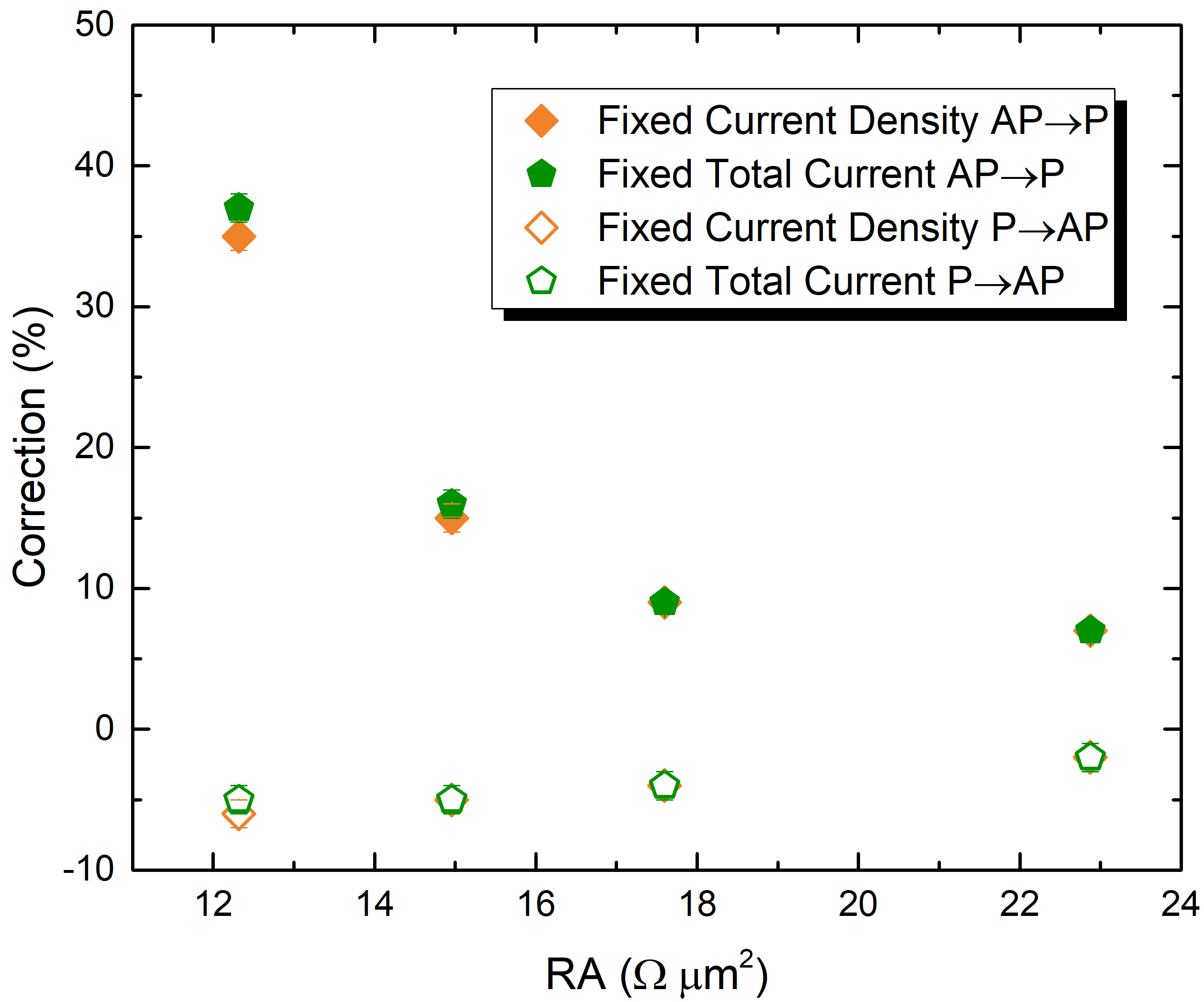
Finally, Fig. 5.16 shows the dependence of the correction on the resistance area (RA) of the structure, achieved by changing the values of both \(R_\text {P}\) and \(R_\text {AP}\),
so as to keep the same TMR. At lower RA values, both the current and the current density increase, leading to much faster switching, which in turn lead to higher values of the current correction required to reproduce the switching
times of the fixed voltage approach. In this case, the dependence of the correction cannot be successfully fitted by a linear regression. The dependence of the correction on both the surface area and the resistance area agrees well
with the previous discussion, as in both cases, when the switching time becomes shorter (for higher surface area and lower RA), the required correction increases.
With an understanding of the behavior of the current correction, it can be applied to allow for the simple constant current density approach to correctly reproduce the switching time distribution, so that it can be employed in place
of more complex and time consuming approaches. The development of a compact model for the correction will thus allow to obtain fast simulation tools for aiding and guiding the design of future devices.